

TMS320C6713B Floating-Point Digital Signal Processor (Rev. A)
TMS320C6713B Floating-Point Digital Signal Processor (Rev. A)
TMS320C6713B Floating-Point Digital Signal Processor (Rev. A)

You also want an ePaper? Increase the reach of your titles
YUMPU automatically turns print PDFs into web optimized ePapers that Google loves.
SPRS294A − OCTOBER 2005 − REVISED NOVEMBER 2005<br />
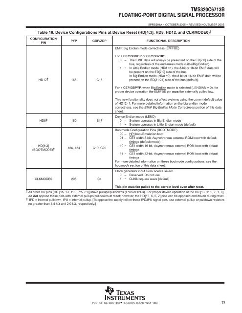
Table 18. Device Configurations Pins at Device Reset (HD[4:3], HD8, HD12, and CLKMODE0) †<br />
CONFIGURATION<br />
PIN<br />
PYP GDP/ZDP FUNCTIONAL DESCRIPTION<br />
EMIF Big Endian mode correctness (EMIFBE)<br />
HD12‡ 168 C15<br />
For a C6713BGDP or C6713BZDP:<br />
0 – The EMIF data will always be presented on the ED[7:0] side of the<br />
bus, regardless of the endianess mode (Little/Big Endian).<br />
1 − In Little Endian mode (HD8 =1), the 8-bit or 16-bit EMIF data will<br />
be present on the ED[7:0] side of the bus.<br />
In Big Endian mode (HD8 =0), the 8-bit or 16-bit EMIF data will be<br />
present on the ED[31:24] side of the bus [default].<br />
For a C6713BPYP, when Big Endian mode is selected (LENDIAN = 0), for<br />
proper device operation the EMIFBE pin must be externally pulled low.<br />
HD8‡ 160 B17<br />
HD[4:3]<br />
(BOOTMODE)‡ 156, 154 C19, C20<br />
CLKMODE0 205 C4<br />
This new functionality does not affect systems using the current default value<br />
of HD12=1. For more detailed information on the big endian mode<br />
correctness, see the EMIF Big Endian Mode Correctness portion of this data<br />
sheet.<br />
Device Endian mode (LEND)<br />
0 – System operates in Big Endian mode<br />
1 − System operates in Little Endian mode (default)<br />
Bootmode Configuration Pins (BOOTMODE)<br />
00 – HPI boot/Emulation boot<br />
01 – CE1 width 8-bit, Asynchronous external ROM boot with default<br />
timings (default mode)<br />
10 − CE1 width 16-bit, Asynchronous external ROM boot with default<br />
timings<br />
11 − CE1 width 32-bit, Asynchronous external ROM boot with default<br />
timings<br />
For more detailed information on these bootmode configurations, see the<br />
bootmode section of this data sheet.<br />
Clock generator input clock source select<br />
0 – Reserved. Do not use.<br />
1 − CLKIN square wave [default]<br />
This pin must be pulled to the correct level even after reset.<br />
† All other HD pins (HD [15, 13, 11:9, 7:5, 2:0]) have pullups/pulldowns (IPUs or IPDs). For proper device operation of the HD [13, 11:9, 7, 1, 0],<br />
do not oppose these pins with external pullups/pulldowns at reset; however, the HD[15, 6, 5, 2] pins can be opposed and driven during reset.<br />
‡ IPD = Internal pulldown, IPU = Internal pullup. [To oppose the supply rail on these IPD/IPU signal pins, use external pullup or pulldown resistors<br />
no greater than 4.4 kΩ and 2.0 kΩ, respectively.]<br />
POST OFFICE BOX 1443 • HOUSTON, TEXAS 77251−1443<br />
33


