

TMS320C6713B Floating-Point Digital Signal Processor (Rev. A)
TMS320C6713B Floating-Point Digital Signal Processor (Rev. A)
TMS320C6713B Floating-Point Digital Signal Processor (Rev. A)

Create successful ePaper yourself
Turn your PDF publications into a flip-book with our unique Google optimized e-Paper software.
SPRS294A − OCTOBER 2005 − REVISED NOVEMBER 2005<br />
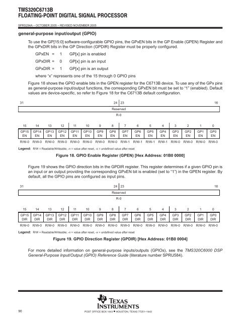
general-purpose input/output (GPIO)<br />
To use the GP[15:0] software-configurable GPIO pins, the GPxEN bits in the GP Enable (GPEN) Register and<br />
the GPxDIR bits in the GP Direction (GPDIR) Register must be properly configured.<br />
GPxEN = 1 GP[x] pin is enabled<br />
GPxDIR = 0 GP[x] pin is an input<br />
GPxDIR = 1 GP[x] pin is an output<br />
where “x” represents one of the 15 through 0 GPIO pins<br />
Figure 18 shows the GPIO enable bits in the GPEN register for the C6713B device. To use any of the GPx pins<br />
as general-purpose input/output functions, the corresponding GPxEN bit must be set to “1” (enabled). Default<br />
values are device-specific, so refer to Figure 18 for the C6713B default configuration.<br />
31 24 23 16<br />
Reserved<br />
R-0<br />
15 14 13 12 11 10 9 8 7 6 5 4 3 2 1 0<br />
GP15<br />
EN<br />
GP14<br />
EN<br />
GP13<br />
EN<br />
GP12<br />
EN<br />
GP11<br />
EN<br />
GP10<br />
EN<br />
GP9<br />
EN<br />
GP8<br />
EN<br />
R/W-0 R/W-0 R/W-0 R/W-0 R/W-0 R/W-0 R/W-0 R/W-0 R/W-1 R/W-1 R/W-1 R/W-1 R/W-0 R/W-0 R/W-0 R/W-0<br />
GP7<br />
EN<br />
Legend: R/W = Readable/Writeable; -n = value after reset, -x = undefined value after reset<br />
GP6<br />
EN<br />
GP5<br />
EN<br />
GP4<br />
EN<br />
GP3<br />
EN<br />
Figure 18. GPIO Enable Register (GPEN) [Hex Address: 01B0 0000]<br />
GP2<br />
EN<br />
GP1<br />
EN<br />
GP0<br />
EN<br />
Figure 19 shows the GPIO direction bits in the GPDIR register. This register determines if a given GPIO pin is<br />
an input or an output providing the corresponding GPxEN bit is enabled (set to “1”) in the GPEN register. By<br />
default, all the GPIO pins are configured as input pins.<br />
31 24 23 16<br />
Reserved<br />
R-0<br />
15 14 13 12 11 10 9 8 7 6 5 4 3 2 1 0<br />
GP15<br />
DIR<br />
GP14<br />
DIR<br />
GP13<br />
DIR<br />
GP12<br />
DIR<br />
GP11<br />
DIR<br />
GP10<br />
DIR<br />
GP9<br />
DIR<br />
GP8<br />
DIR<br />
R/W-0 R/W-0 R/W-0 R/W-0 R/W-0 R/W-0 R/W-0 R/W-0 R/W-0 R/W-0 R/W-0 R/W-0 R/W-0 R/W-0 R/W-0 R/W-0<br />
GP7<br />
DIR<br />
Legend: R/W = Readable/Writeable; -n = value after reset, -x = undefined value after reset<br />
GP6<br />
DIR<br />
GP5<br />
DIR<br />
GP4<br />
DIR<br />
GP3<br />
DIR<br />
Figure 19. GPIO Direction Register (GPDIR) [Hex Address: 01B0 0004]<br />
GP2<br />
DIR<br />
GP1<br />
DIR<br />
GP0<br />
DIR<br />
For more detailed information on general-purpose inputs/outputs (GPIOs), see the TMS320C6000 DSP<br />
General-Purpose Input/Output (GPIO) Reference Guide (literature number SPRU584).<br />
90 POST OFFICE BOX 1443 • HOUSTON, TEXAS 77251−1443


