Semiconductor Equipment - Berenberg Bank
Semiconductor Equipment - Berenberg Bank
Semiconductor Equipment - Berenberg Bank

You also want an ePaper? Increase the reach of your titles
YUMPU automatically turns print PDFs into web optimized ePapers that Google loves.
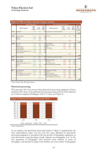
Tokyo Electron Ltd<br />
Technology Hardware<br />
Figure 4: TEL is mainly exposed to legacy markets<br />
Market exposure<br />
High Growth markets<br />
2012-<br />
2017<br />
CAGR<br />
% of<br />
revenue<br />
2012<br />
market<br />
share<br />
Low Growth/Declining markets<br />
Market exposure<br />
ASML Lithograhy +18% 100% 74% no exposure to low growth market<br />
2012-<br />
2017<br />
CAGR<br />
% of<br />
revenue<br />
2012<br />
market<br />
share<br />
2012-<br />
2017<br />
Growth<br />
CAGR<br />
18.0%<br />
ASMI ALD deposition +15.0% 60% 45% LP CVD 1.0% 9% 51%<br />
Epitaxy +7.5% 17% 9%<br />
PE CVD +5.0% 14% 9%<br />
91% 9%<br />
AMAT PE CVD +5.0% 19% 47% Ion implanter -2.5% 11% 76%<br />
Epitaxy +8.0% 11% 89% Dielectric etching 0.5% 1% 5%<br />
Silicon etching +4.0% 8% 14% PVD 0.0% 21% 78%<br />
CMP&cleaning +3.0% 6% 59% RTP Thermal -3.0% 7% 42%<br />
Process control +6.0% 9% 76%<br />
Wafer level packaging excl conta +12.0% 6% 9%<br />
Fab automation +4.0% 3% 16%<br />
61% 39%<br />
KLA process control +6.0% 100% 54% no exposure to low growth market<br />
LAM Silicon etching +4.0% 50% 59% Dielectric etching 0.5% 14% 26%<br />
Metal etching +6.0% 4% LP CVD 1.0% 3% 10%<br />
Wafer level packaging excl conta +12.0% 1% Bevel edge removal -2.4% 3% 100%<br />
PE CVD +5.0% 15% 40% Cleaning (spin.spray processor) -2.0% 6% 15%<br />
ECD +4.0% 4%<br />
74% 26%<br />
TEL ALD deposition +15.0% 6% 44% Photoresist processing 1.4% 34% 89%<br />
Silicon etch +4.0% 8% 9% LP CVD 1.0% 12% 51%<br />
WL packaging-excl contact prob +12.0% 5% 3% Dielectric etching 0.5% 20% 63%<br />
WL packaging- contact prob +3.0% 4% 39% RTP oxidisation/diffusion -1.5% 3% 22%<br />
Cleaning (spin.spray processor) -2.0% 9% 13%<br />
23% 77%<br />
11.1%<br />
3.3%<br />
6.0%<br />
3.2%<br />
2.4%<br />
Source: Gartner Data, <strong>Berenberg</strong> estimates<br />
Photoresist processing<br />
TEL generates 34% of its revenue from photoresist processing equipment. It had a<br />
dominant, 89% share of the global photoresist processing market in 2012, followed<br />
by its closest competitor Dainippon, with a 7% share (see Figure 5).<br />
Figure 5: Photoresist processing market share<br />
100%<br />
90%<br />
80%<br />
70%<br />
60%<br />
50%<br />
40%<br />
30%<br />
20%<br />
10%<br />
0%<br />
2010 2011 2012<br />
Source: Gartner Data<br />
TEL Dainippon SEMES Suss FSI<br />
In our opinion, the photoresist processing market is likely to underperform the<br />
total semiconductor capex over the next few years. Demand for photoresist<br />
processing equipment is associated with unit growth of lithography equipment, as<br />
each photoresist coater/developer usually supports one lithography tool. As the<br />
new generation of lithography tools becomes more efficient in terms of<br />
throughput, and demand for legacy tools declines, the total number of lithography<br />
122