Semiconductor Equipment - Berenberg Bank
Semiconductor Equipment - Berenberg Bank
Semiconductor Equipment - Berenberg Bank

Create successful ePaper yourself
Turn your PDF publications into a flip-book with our unique Google optimized e-Paper software.
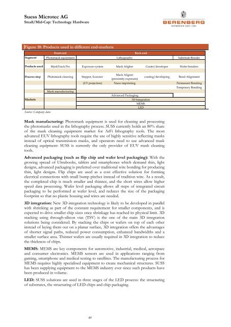
Suess Microtec AG<br />
Small/Mid-Cap: Technology Hardware<br />
Figure 10: Products used in different end-markets<br />
Front end<br />
Back end<br />
Segment Photomask equipment Lithography<br />
Substrate Bonder<br />
Products used MaskTrack Pro Exposure system Mask Aligher Coater/developer Wafer bonders<br />
Process step Photomask cleaning Stepper, Scanner<br />
Mask Aligner<br />
(proximity exposure)<br />
coating/developing Bond Alignment<br />
(UV projection) Nano imprinting Permanent Bonding<br />
Temporary Bonding<br />
Mask manufacturing<br />
Advanced Packaging<br />
Markets<br />
3D Integration<br />
MEMS<br />
LED<br />
Source: Company data<br />
Mask manufacturing: Photomask equipment is used for cleaning and processing<br />
the photomasks used in the lithography process. SUSS currently holds an 80% share<br />
of the mask cleaning equipment market for ArFi lithography tools. The most<br />
advanced EUV lithography tools require the use of highly sensitive reflecting masks<br />
instead of optical transmission masks, and operators need to use advanced mask<br />
cleaning equipment: SUSS is currently the only provider of EUV mask cleaning<br />
tools.<br />
Advanced packaging (such as flip chip and wafer level packaging): With the<br />
growing spread of Ultrabooks, tablets and smartphones which demand thin, light<br />
designs, advanced packaging is preferred over traditional wire bonding for producing<br />
thin, light designs. Flip chips are used as a cost effective solution for forming<br />
electrical connections with small bump pitches instead of tradition wire. As a result,<br />
the completed chip is much smaller and thinner, and the short wires allow higher<br />
speed data processing. Wafer level packaging allows all steps of integrated circuit<br />
packaging to be performed at wafer level, and reduces the size of the packaging<br />
footprint so that no plastic housing and wires are needed.<br />
3D integration: New 3D integration technology is likely to be developed in parallel<br />
with shrinking as part of the constant requirement for smaller components, and is<br />
expected to drive smaller chip sizes once shrinkage has reached its physical limit. 3D<br />
stacking using through-silicon vias (TSV) is the one of the main 3D integration<br />
solutions being considered. By stacking the chips or wafers on top of each other<br />
instead of laying them out on a planar surface, 3D integration offers the advantages<br />
of shorter signal paths, reduced power consumption, enhanced bandwidths and a<br />
smaller surface area. Thinner wafers are usually required in 3D integration to reduce<br />
the thickness of chips.<br />
MEMS: MEMS are key components for automotive, industrial, medical, aerospace<br />
and consumer electronics. MEMS sensors are used in applications ranging from<br />
gaming, smartphone and medical testing to satellites. The manufacturing process for<br />
MEMS requires highly specialised equipment to create mechanical structures. SUSS<br />
has been supplying equipment to the MEMS industry ever since such products have<br />
been produced in volume.<br />
LED: SUSS solutions are used in three stages of the LED process: the structuring<br />
of substrates, the structuring of LED chips and chip packaging.<br />
87