Semiconductor Equipment - Berenberg Bank
Semiconductor Equipment - Berenberg Bank
Semiconductor Equipment - Berenberg Bank

Create successful ePaper yourself
Turn your PDF publications into a flip-book with our unique Google optimized e-Paper software.
Tokyo Electron Ltd<br />
Technology Hardware<br />
tools is likely to grow at a slower pace. Gartner forecasts the photoresist<br />
processing market will grow by c1.4% between 2012 and 2017, versus growth in<br />
semiconductor capex of c4.1%.<br />
In 2015-16, when extreme ultraviolet lithography (EUV) starts to ship in volume,<br />
we may potentially see a higher top-line growth rate. The photoresist used for<br />
EUV is different from conventional lithography tools and requires a different type<br />
of photoresist equipment which may carry a high ASP. However, there is little<br />
visibility on revenue upside.<br />
Etching<br />
TEL generates 27% of its revenue from etching equipment, with a 29% market<br />
share globally in 2012. Some 85% of TEL’s etching revenue comes from shipping<br />
dielectric etching equipment, with the remainder from silicon etching equipment. It<br />
holds a dominant 63% share in the dielectric etching market, and a 9% share in<br />
silicon etching (LAM leads this market with a 59% share).<br />
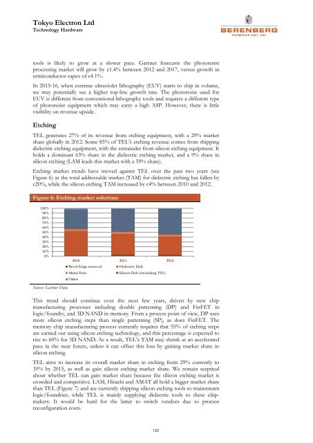
Etching market trends have moved against TEL over the past two years (see<br />
Figure 6) as the total addressable market (TAM) for dielectric etching has fallen by<br />
c20%, while the silicon etching TAM increased by c4% between 2010 and 2012.<br />
Figure 6: Etching market solutions<br />
100%<br />
90%<br />
80%<br />
70%<br />
60%<br />
50%<br />
40%<br />
30%<br />
20%<br />
10%<br />
0%<br />
Source: Gartner Data<br />
2010 2011 2012<br />
Bevel Edge removal Dielectric Etch<br />
Metal Etch<br />
Other<br />
Silicon Etch (including TSV)<br />
This trend should continue over the next few years, driven by new chip<br />
manufacturing processes including double patterning (DP) and FinFET in<br />
logic/foundry, and 3D NAND in memory. From a process point of view, DP uses<br />
more silicon etching steps than single patterning (SP), as does FinFET. The<br />
memory chip manufacturing process currently requires that 55% of etching steps<br />
are carried out using silicon etching technology, and this percentage is expected to<br />
rise to 60% for 3D NAND. As a result, TEL’s TAM may shrink at an accelerated<br />
pace in the near future, unless it can offset this loss by gaining market share in<br />
silicon etching.<br />
TEL aims to increase its overall market share in etching from 29% currently to<br />
35% by 2015, as well as gain silicon etching market share. We remain sceptical<br />
about whether TEL can gain market share because the silicon etching market is<br />
crowded and competitive. LAM, Hitachi and AMAT all hold a bigger market share<br />
than TEL (Figure 7) and are currently shipping silicon etching tools to mainstream<br />
logic/foundries, while TEL is mainly supplying dielectric tools to these chipmakers.<br />
It would be hard for the latter to switch vendors due to process<br />
reconfiguration costs.<br />
123