Semiconductor Equipment - Berenberg Bank
Semiconductor Equipment - Berenberg Bank
Semiconductor Equipment - Berenberg Bank

You also want an ePaper? Increase the reach of your titles
YUMPU automatically turns print PDFs into web optimized ePapers that Google loves.
<strong>Semiconductor</strong> <strong>Equipment</strong><br />
Technology Hardware<br />
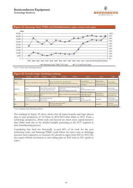
Figure 21: Samsung, Intel, TSMC and Globalfoundries capex versus total capex<br />
$mn<br />
45,000<br />
40,000<br />
35,000<br />
30,000<br />
25,000<br />
20,000<br />
15,000<br />
10,000<br />
5,000<br />
0<br />
1999 2000 2001 2002 2003 2004 2005 2006 2007 2008 2009 2010 2011 2012 2013E2014E2015E2016E<br />
100%<br />
90%<br />
80%<br />
70%<br />
60%<br />
50%<br />
40%<br />
30%<br />
20%<br />
10%<br />
0%<br />
Source: Gartner data, <strong>Berenberg</strong> estimates<br />
Samsung, Intel, TSMC, GF Capex<br />
% of total semi capex<br />
Figure 22: Foundry/logic shrinking roadmap<br />
Foundry/Logic<br />
H1 2010 H2 2010 H1 2011 H2 2011 H1 2012 H2 2012 2013E 2014E 2015E<br />
TSMC<br />
-40/65nm contribute 53% revenue in 2010,<br />
-28nm started Q3 2011, 22% Q4 2012 rev<br />
-28nm good yield in HKMG & Poly SiON at 2012 end,<br />
-expand 28nm,<br />
-28nm mature,<br />
-20nm & 16nm FinFET risk - 20nm/16nm start<br />
production,<br />
volume production,<br />
-20nm/16nm,<br />
-10nm FInFET R&D.<br />
Samsung<br />
UMC<br />
GF<br />
Intel<br />
-40nm<br />
-65nm&finer eqv 35% rev, - 40nm eqv 10% above rev in Q4<br />
-40nm eqv low single digit. 2011,<br />
- 45nm,<br />
-started 32nm at 2010 end.<br />
-32nm<br />
-32nm HKMG started in 2011,<br />
-45/32nm supply constrain,<br />
-32nm yileld improved,<br />
-45nm/32nm<br />
-22nm 3D, main node in 2013<br />
-start 14nm end of 2013<br />
-started 28nm started with good yield<br />
in 2012 end,<br />
-28nm both HKMG & Poly SiON<br />
-28nm start, contribute low<br />
-28nm&20nm,<br />
-40nm contribute 15% revenue by 2012 esingle digit % by YE,<br />
-14nm tape out.<br />
mainly Poly SiON<br />
-28nm started and<br />
good yield at year<br />
end,<br />
-20nm<br />
-start 14nmFinFET in 2013<br />
-20nm,<br />
-develop 14nm XM<br />
-14nmXM<br />
-14nm 3D<br />
-20nm/14nm<br />
-10nm FInFET R&D<br />
-14nm FinFET risk<br />
production start<br />
-20nm/14nm,<br />
-10nm FInFET R&D.<br />
-10nm 3D,<br />
-next 7nm and 5nm<br />
Source: Company data, <strong>Berenberg</strong> estimates<br />
The roadmap in Figure 22 above shows that all major foundry and logic players<br />
plan to start production of 16/10nm in 2014/2015 after 20nm in 2013. From a<br />
technology perspective, 20nm node and beyond are much more capital-intensive<br />
than 28nm node due to the double/multiple patterning or the EUV required in<br />
their manufacturing process.<br />
Considering that Intel has historically re-used 80% of its tools for the next<br />
technology node, and Samsung/TSMC could follow the same route as shrinkage<br />
becomes more expensive, we forecast c3% growth in capex from 2013 to 2015. We<br />
also expect 450mm investment to start taking place in 2016 with an 18% uptick in<br />
capex.<br />
20