Semiconductor Equipment - Berenberg Bank
Semiconductor Equipment - Berenberg Bank
Semiconductor Equipment - Berenberg Bank

You also want an ePaper? Increase the reach of your titles
YUMPU automatically turns print PDFs into web optimized ePapers that Google loves.
ASML Holding NV<br />
Technology Hardware<br />
Lithography market to double in size by 2016<br />
Consumer electronics will be the main driver of semiconductor growth in the next<br />
few years, in our opinion. Chip-makers are actively scaling their chip sizes down to<br />
facilitate the new generation of device designs, which are smaller, lighter, more<br />
power-efficient and have better performance. As shown in Figure 9 below, all the<br />
major chip-makers are planning to enter lithography-intensive 20nm/10nm node<br />
in 2013/2014, and then expand their leading-edge chip output afterwards. As chipmakers<br />
shrink down the technology roadmap, they require more lithography tools<br />
which can print to smaller nodes.<br />
Figure 9: Chip-maker roadmap<br />
2010 2011 2012<br />
2013E 2014E 2015E<br />
Foundry/Logic<br />
TSMC<br />
-40/65nm<br />
-28nm HKMG & Poly SiON<br />
-28nm/20nm/16nm FinFET -28nm/20nm/16nm -20nm/16nm/10nm FinFET<br />
Samsung -40nm -45/32nm HKMG -28nm HKMG & Poly SiON -20nm<br />
-20nm/14nm/10nm FinFET<br />
UMC -65nm/40nm - 40nm -40nm<br />
-28nm Poly SiON -28nm/20nm/14nm -14nm FinFET<br />
GF - 45nm/ 32nm 45nm/32nm<br />
-28nm -20nm/14nm XM -14nmXM -20nm/14nm/10nm FinFET<br />
Intel -32nm -22nm 3D, 14nm end of 2013<br />
-14nm 3D -10nm 3D/7nm/5nm<br />
NAND<br />
Samsung -27nm -21nm<br />
-19nm -19nm/16nm -16nm -12nm/14nm/3D NAND<br />
Toshiba/SanDisk -24nm -19nm<br />
-19nm/3D NAND. -16nm -12nm/14nm/3D NAND<br />
Micron(Elpida)<br />
- 25nm -20nm -1Y(18/15nm)/3D NAND -16nm/14nm/12nm/3D NAND<br />
SK Hynix<br />
-26nm -20nm - 16nm/3D NAND -14nm/12nm/3D NAND<br />
DRAM<br />
Samsung - 40nm -40nm/35nm/28nm -25nm - 2Y(23nm/25nm)/28nm<br />
-2Ynm & 2Znm (20/21nm).<br />
Micron -50nm -32nm<br />
-24nm<br />
- 24nm/2Znm<br />
Elpida<br />
SK Hynix<br />
-42nm<br />
-44nm<br />
-32nm<br />
-40nm/38nm<br />
-25nm<br />
-3xnm/28nm/23nm<br />
Others<br />
-45nm/42nm/30nm -30nm&2xnm<br />
Source: Company data, <strong>Berenberg</strong> estimate<br />
Source: Company data, <strong>Berenberg</strong> estimates<br />
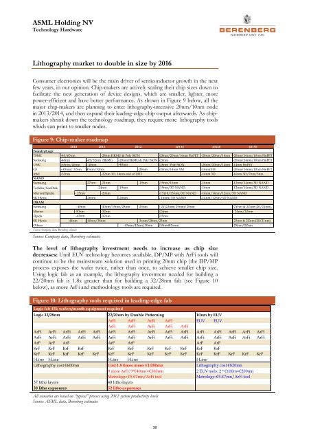
The level of lithography investment needs to increase as chip size<br />
decreases: Until EUV technology becomes available, DP/MP with ArFi tools will<br />
continue to be the mainstream solution used in printing 20nm chip (the DP/MP<br />
process exposes the wafer twice, rather than once, to achieve smaller chip size.<br />
Using logic fab as an example, the lithography investment needed for building a<br />
22/20nm fab is 1.8x greater than for building a 32/28nm fab (see Figure 10<br />
below), as more ArFi and methodology tools are required.<br />
Figure 10: Lithography tools required in leading-edge fab<br />
All scenarios are based on “typical” process using 2012 system productivity levels<br />
Source: ASML data, <strong>Berenberg</strong> estimates<br />
-23nm & 2Znm (20/21nm)<br />
-2Xnm/2Znm<br />
Logic fab 45k wafers/month equipment required<br />
Logic 32/28nm 22/20nm by Double Patterning 10nm by EUV<br />
ArFi ArFi ArFi ArFi EUV EUV<br />
ArFi ArFi ArFi ArFi ArFi<br />
ArFi ArFi ArFi ArFi ArFi ArFi ArFi ArFi ArFi ArFi ArFi ArFi ArFi ArFi ArFi<br />
ArFi ArFi ArFi ArFi ArFi ArFi ArFi ArFi ArFi ArFi ArFi ArFi ArFi ArFi ArFi<br />
ArF ArF ArF ArF ArF ArF ArF<br />
KrF KrF KrF KrF KrF KrF KrF KrF KrF KrF KrF<br />
KrF KrF KrF KrF KrF KrF KrF KrF KrF KrF KrF KrF KrF KrF KrF<br />
I-Line I-Line I-Line I-Line I-Line<br />
Lithography cost €600mn Cost 1.8 times more: €1,080mn Lithography cost €820mn<br />
9 more ArFi: 9*€40mn=€360mn 2 EUV tools: 2 * €100m=€200mn<br />
Metrology: €5-€7mn/ArFi tool<br />
Metrology: €5-€7mn/ArFi tool<br />
37 litho layers 40 litho layers<br />
38 litho exposures 52 litho exposures<br />
38