Semiconductor Equipment - Berenberg Bank
Semiconductor Equipment - Berenberg Bank
Semiconductor Equipment - Berenberg Bank

You also want an ePaper? Increase the reach of your titles
YUMPU automatically turns print PDFs into web optimized ePapers that Google loves.
<strong>Semiconductor</strong> <strong>Equipment</strong><br />
Technology Hardware<br />
We believe the lithography, process control, and wafer level packaging markets<br />
have the biggest growth potential, driven by node shrinkage and 3D packaging<br />
demand, hence ASML, KLA and SUSS are likely to outperform other equipment<br />
suppliers. We do not like the etching, deposition and die level packaging markets<br />
because their growth potential is limited as a result of technology migration.<br />
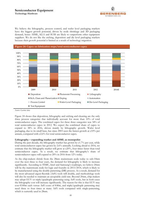
Figure 24: Capex on fabrication steps/total semiconductor capex<br />
100%<br />
90%<br />
80%<br />
70%<br />
60%<br />
50%<br />
40%<br />
30%<br />
20%<br />
10%<br />
0%<br />
2009 2010 2011 2012 2016E<br />
Deposition Photoresist Processing Lithography<br />
Etch, Clean and Planarization Doping Automation<br />
Process Control Wafer-Level Packaging Die-Level Packaging<br />
Test <strong>Equipment</strong><br />
Source: Gartner data<br />
Figure 24 shows that deposition, lithography and etching and cleaning are the only<br />
three process categories that individually account for more than 10% of total<br />
semiconductor capex. The combined capex for these three categories was 34% of<br />
total semiconductor capex in 2012. We expect the combined share of capex to<br />
expand to 38% in 2016, driven mainly by lithography growth. Wafer level<br />
packaging, due to its small base, has since 2003 seen the fastest growth at c10% per<br />
annum, compared with c2.6% for total semiconductor capex.<br />
Lithography – expanding market and ASML as monopolist<br />
During the past decade, the lithography market has grown by c1.7% per year, while<br />
total semiconductor capex has grown by 2.6% annually. Looking ahead to 2016, we<br />
estimate that the lithography market will grow at c20%, four times faster than total<br />
semiconductor capex. At a result, we estimate that lithography’s share of<br />
semiconductor capex will expand to 20% in 2016 from 12% today.<br />
As the chip-makers shrink from the 28nm mainstream node today to sub-10nm<br />
over the next three to four years, the demand for lithography is likely to increase<br />
significantly. According to TSMC, Intel and Samsung’s roadmaps, we believe 20nm<br />
will be the mainstream node for logic and foundry in 2013/2014, which is likely to<br />
be manufactured using the double patterning (DB) process. As a result, demand for<br />
the most advanced argon-fluoride (ArFi) tools will double, and methodology tools<br />
will also be needed to maintain an acceptable yield rate. Beyond 20nm, chip-makers<br />
may adopt EUV or triple/quadruple patterning using ArFi tools, but in both cases<br />
the lithography cost will increase significantly. The reason for this is that EUV may<br />
cost €100m each versus ArFi costs of €40m, and triple/quadruple patterning may<br />
need three to four times as many ArFi tools compared with single-patterning,<br />
which is currently used in 28nm.<br />
22