Semiconductor Equipment - Berenberg Bank
Semiconductor Equipment - Berenberg Bank
Semiconductor Equipment - Berenberg Bank

Create successful ePaper yourself
Turn your PDF publications into a flip-book with our unique Google optimized e-Paper software.
<strong>Semiconductor</strong> <strong>Equipment</strong><br />
Technology Hardware<br />
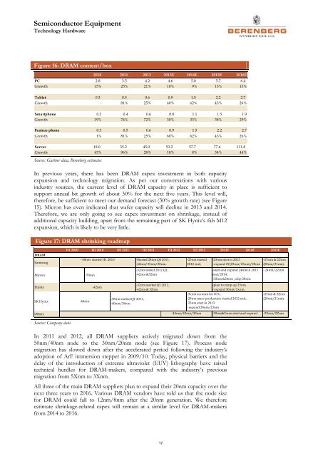
Figure 16: DRAM content/box<br />
2010 2011 2012 2013E 2014E 2015E 2016E<br />
PC 2.8 3.5 4.2 4.6 5.0 5.7 6.4<br />
Growth 15% 25% 21% 10% 9% 13% 13%<br />
Tablet 0.3 0.5 0.6 0.9 1.5 2.2 2.7<br />
Growth - 81% 25% 60% 62% 43% 26%<br />
Smartphone 0.2 0.4 0.6 0.8 1.1 1.5 1.9<br />
Growth 19% 74% 72% 30% 33% 38% 29%<br />
Featrue phone 0.3 0.5 0.6 0.9 1.5 2.2 2.7<br />
Growth 1% 81% 25% 60% 62% 43% 26%<br />
Server 18.0 35.2 45.0 53.2 57.7 77.6 111.8<br />
Growth 43% 96% 28% 18% 8% 34% 44%<br />
Source: Gartner data, <strong>Berenberg</strong> estimates<br />
In previous years, there has been DRAM capex investment in both capacity<br />
expansion and technology migration. As per our conversations with various<br />
industry sources, the current level of DRAM capacity in place is sufficient to<br />
support annual bit growth of about 30% for the next five years. This level will,<br />
therefore, be sufficient to meet our demand forecast (30% growth rate) (see Figure<br />
15). Micron has even indicated that wafer capacity will decline in 2013 and 2014.<br />
Therefore, we are only going to see capex investment on shrinkage, instead of<br />
additional capacity building, apart from the remaining part of SK Hynix’s fab M12<br />
expansion, which is likely to be very little.<br />
Figure 17: DRAM shrinking roadmap<br />
DRAM<br />
Samsung<br />
Micron<br />
H1 2010 H2 2010 H1 2011 H2 2011 H1 2012 H2 2012 2013E 2014E 2015E<br />
- 40nm started H1 2010 -Started 28nm Q4 2011,<br />
-40nm/35nm/28nm.<br />
-32nm stated 2012 Q1,<br />
-50nm<br />
-42nm &32nm<br />
-25nm started<br />
2012 end,<br />
-23nm start in 2013<br />
- expand 2Y(23nm/25nm)/28nm<br />
-start and expand 24nm in 2013<br />
end/2014,<br />
-32nm &24nm , skip 28nm.<br />
-2Ynm & 2Znm<br />
(20nm/21nm).<br />
- 24nm/2Znm<br />
Elpida<br />
SK Hynix<br />
-44nm<br />
-42nm<br />
-38nm started Q1 2011,<br />
-40nm/38nm<br />
-32nm started Q1 2012,<br />
-42nm & 32nm.<br />
-plan to ramp up 25nm,<br />
- expand 30nm/2xnm.<br />
-3xnm account for 70%,<br />
-28nm mass production started 2012 end,<br />
-23nm start in 2013<br />
- expand 28nm/23nm<br />
-23nm & 2Znm<br />
(20nm/21nm).<br />
Others<br />
-45nm/42nm/30nm<br />
-30nm&2xnm start and expand<br />
-2Xnm/2Znm<br />
Source: Company data<br />
In 2011 and 2012, all DRAM suppliers actively migrated down from the<br />
50nm/40nm node to the 30nm/20nm node (see Figure 17). Process node<br />
migration has slowed down after the accelerated period following the industry’s<br />
adoption of ArF immersion stepper in 2009/10. Today, physical barriers and the<br />
delay of the introduction of extreme ultraviolet (EUV) lithography have raised<br />
technical hurdles for DRAM-makers, compared with the industry’s previous<br />
migration from 5Xnm to 3Xnm.<br />
All three of the main DRAM suppliers plan to expand their 20nm capacity over the<br />
next three years to 2016. Various DRAM vendors have told us that the node size<br />
for DRAM could fall to 12nm/8nm after the 20nm generation. We therefore<br />
estimate shrinkage-related capex will remain at a similar level for DRAM-makers<br />
from 2014 to 2016.<br />
17