Semiconductor Equipment - Berenberg Bank
Semiconductor Equipment - Berenberg Bank
Semiconductor Equipment - Berenberg Bank

You also want an ePaper? Increase the reach of your titles
YUMPU automatically turns print PDFs into web optimized ePapers that Google loves.
<strong>Semiconductor</strong> <strong>Equipment</strong><br />
Technology Hardware<br />
Figure 29 shows that LAM dominates the etching market, with a 47% market share<br />
in 2012, followed by TEL, with a share of 29%. TEL may lose share in etching due<br />
to its focus on the low-growth dielectric etching market. AMAT has a 10% market<br />
share of the etching market. In 2011 and 2012, it lost 9% of its market share in the<br />
etching market, from both dielectric and silicon etching. In our opinion, winning<br />
back the lost share from LAM and Hitachi will not be easy.<br />
In the etching market, we think LAM will outperform as it has the greatest share in<br />
silicon etching. We think TEL will underperform because of its heavy exposure to<br />
dielectric etching (63% share). AMAT has a 10% share of the etching market. It<br />
generates more revenue from silicon etching than dielectric etching, and has a<br />
higher market share in silicon etching.<br />
Wafer level packaging<br />
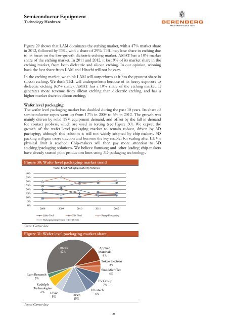
The wafer level packaging market has doubled during the past 10 years. Its share of<br />
semiconductor capex went up from 1.7% in 2004 to 3% in 2012. The growth was<br />
mainly driven by solid TSV equipment demand, and offset by the fall in demand<br />
for contact probers, which are used in testing (see Figure 30). We expect the<br />
growth of the wafer level packaging market to remain robust, driven by 3D<br />
packaging, although this solution is still not widely adopted by chip-makers. 3D<br />
packing will gain more traction and become the key enabler for scaling after EUV’s<br />
physical limit is reached. Chip-makers will then pay more attention to 3D<br />
stacking/packaging solutions. We believe Samsung and other leading chip-makers<br />
have already started pilot production lines using 3D packaging technology.<br />
Figure 30: Wafer level packaging market trend<br />
Wafer Level Packaging market by Solution<br />
40%<br />
35%<br />
30%<br />
25%<br />
20%<br />
15%<br />
10%<br />
5%<br />
0%<br />
2008 2009 2010 2011 2012<br />
Litho Tool TSV Tool Bump Processing<br />
Packaging inspection<br />
Others<br />
Source: Gartner data<br />
Figure 31: Wafer level packaging market share<br />
Lam Research<br />
3%<br />
Rudolph<br />
Technologies<br />
6% Ulvac<br />
5%<br />
Source: Gartner data<br />
Others<br />
42%<br />
Disco<br />
15%<br />
Applied<br />
Materials<br />
9%<br />
Tokyo Electron<br />
3%<br />
Suss MicroTec<br />
4%<br />
EV Group<br />
7%<br />
Ultratech<br />
6%<br />
26