Semiconductor Equipment - Berenberg Bank
Semiconductor Equipment - Berenberg Bank
Semiconductor Equipment - Berenberg Bank

Create successful ePaper yourself
Turn your PDF publications into a flip-book with our unique Google optimized e-Paper software.
<strong>Semiconductor</strong> <strong>Equipment</strong><br />
Technology Hardware<br />
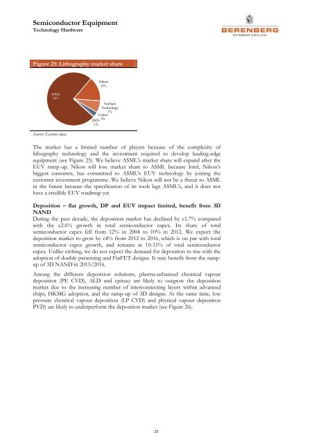
Figure 25: Lithography market share<br />
Nikon<br />
15%<br />
ASML<br />
74%<br />
NuFlare<br />
Technology<br />
7%<br />
Canon<br />
3%<br />
JEOL<br />
1%<br />
Source: Gartner data<br />
The market has a limited number of players because of the complexity of<br />
lithography technology and the investment required to develop leading-edge<br />
equipment (see Figure 25). We believe ASML’s market share will expand after the<br />
EUV ramp-up. Nikon will lose market share to ASML because Intel, Nikon’s<br />
biggest customer, has committed to ASML’s EUV technology by joining the<br />
customer investment programme. We believe Nikon will not be a threat to ASML<br />
in the future because the specification of its tools lags ASML’s, and it does not<br />
have a credible EUV roadmap yet.<br />
Deposition – flat growth, DP and EUV impact limited, benefit from 3D<br />
NAND<br />
During the past decade, the deposition market has declined by c1.7% compared<br />
with the c2.6% growth in total semiconductor capex. Its share of total<br />
semiconductor capex fell from 12% in 2004 to 10% in 2012. We expect the<br />
deposition market to grow by c4% from 2012 to 2016, which is on par with total<br />
semiconductor capex growth, and remains at 10-11% of total semiconductor<br />
capex. Unlike etching, we do not expect the demand for deposition to rise with the<br />
adoption of double patterning and FinFET designs. It may benefit from the rampup<br />
of 3D NAND in 2015/2016.<br />
Among the different deposition solutions, plasma-enhanced chemical vapour<br />
deposition (PE CVD), ALD and epitaxy are likely to outgrow the deposition<br />
market due to the increasing number of interconnecting layers within advanced<br />
chips, HKMG adoption, and the ramp-up of 3D designs. At the same time, low<br />
pressure chemical vapour deposition (LP CVD) and physical vapour deposition<br />
PVD) are likely to underperform the deposition market (see Figure 26).<br />
23