Semiconductor Equipment - Berenberg Bank
Semiconductor Equipment - Berenberg Bank
Semiconductor Equipment - Berenberg Bank

You also want an ePaper? Increase the reach of your titles
YUMPU automatically turns print PDFs into web optimized ePapers that Google loves.
ASML Holding NV<br />
Technology Hardware<br />
EUV drives ASML’s future success<br />
EUV is the key enabler of Moore’s law, and ASML holds 100%<br />
market share<br />
<strong>Semiconductor</strong> manufacturing is driven by Moore’s law, which states that the<br />
number of transistors on an affordable chip will double every two years. As chipmakers<br />
start to print 20nm chips, and subsequently 10nm, 7nm and 5nm chips, the<br />
EUV solution is both cheaper and simpler than ArFi solutions. ASML’s coinvestment<br />
programme demonstrated the commitment from Intel, Samsung and<br />
TSMC to this technology, and ASML is recognised as technology leader in this<br />
field.<br />
The DP/multi-patterning (MP) process using ArFi tools (which exposes the wafer<br />
twice instead of once in order to reduce the printed feature size) is now the<br />
mainstream solution for printing 20nm chips. However, manufacturers claim that<br />
this process is too costly because it increases the number of lithography exposures<br />
per wafer, meaning that they must either reduce output or buy more tools. EUV<br />
enables chip-makers to expose the critical layer in just one exposure instead of two.<br />
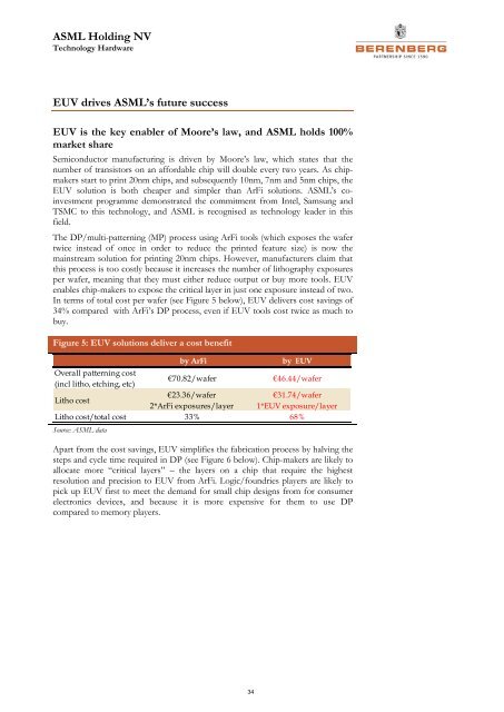
In terms of total cost per wafer (see Figure 5 below), EUV delivers cost savings of<br />
34% compared with ArFi’s DP process, even if EUV tools cost twice as much to<br />
buy.<br />
Figure 5: EUV solutions deliver a cost benefit<br />
by ArFi<br />
by EUV<br />
Overall patterning cost<br />
(incl litho, etching, etc)<br />
€70.82/wafer<br />
€46.44/wafer<br />
Litho cost<br />
€23.36/wafer<br />
€31.74/wafer<br />
2*ArFi exposures/layer 1*EUV exposure/layer<br />
Litho cost/total cost 33% 68%<br />
Source: ASML data<br />
Apart from the cost savings, EUV simplifies the fabrication process by halving the<br />
steps and cycle time required in DP (see Figure 6 below). Chip-makers are likely to<br />
allocate more “critical layers” – the layers on a chip that require the highest<br />
resolution and precision to EUV from ArFi. Logic/foundries players are likely to<br />
pick up EUV first to meet the demand for small chip designs from for consumer<br />
electronics devices, and because it is more expensive for them to use DP<br />
compared to memory players.<br />
34