Semiconductor Equipment - Berenberg Bank
Semiconductor Equipment - Berenberg Bank
Semiconductor Equipment - Berenberg Bank

You also want an ePaper? Increase the reach of your titles
YUMPU automatically turns print PDFs into web optimized ePapers that Google loves.
<strong>Semiconductor</strong> <strong>Equipment</strong><br />
Technology Hardware<br />
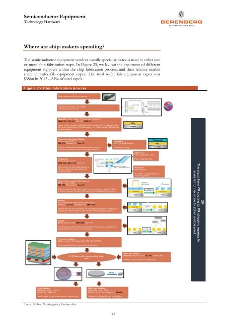
Where are chip-makers spending?<br />
The semiconductor equipment vendors usually specialise in tools used in either one<br />
or more chip fabrication steps. In Figure 23, we lay out the exposures of different<br />
equipment suppliers within the chip fabrication process, and their relative market<br />
share in wafer fab equipment capex. The total wafer fab equipment capex was<br />
$38bn in 2012 – 81% of total capex.<br />
Figure 23: Chip fabrication process<br />
Silicon ingots up to 300mm in diameter<br />
Ingots sliced into wafer and polished<br />
ShinEtsu, Sumco, Siltronic<br />
Deposition: $6bn market (15.7% total semi equipment)<br />
AMAT 47%, TEL 12%, LAM 11%, ASMI 5%<br />
Grows, coats or transfer a material onto wafer, known as thin film deposition. Eg:<br />
SiO 2 which is widely used. (the yellow layer in pic) Performed by CVD/Pasma/PVD<br />
treatment systems.<br />
Si Wafer<br />
Photoresist processing - Coating:<br />
$1.6bn market (4.2%)<br />
TEL 89%, Dainippon 7%, Suss 1%<br />
Wafer is coated with chemical photoresist, thus pattern on<br />
photomask transferred to wafer surface after exposure.<br />
Photoresist:<br />
JSR, TOK,RHEM,ShinEtsu<br />
Chemical photoresist.<br />
SiO 2<br />
SiO 2<br />
Photoresist<br />
Lightsource:<br />
Cymer, Gigaphoton, Ushio<br />
Si Wafer<br />
Lithography:<br />
$6.5bn market (17.2%)<br />
ASML 74%, Nikon 17%, Canon 2%<br />
Wafer coated with photoresist exposed by<br />
litho tool (machine focuses, aligns, and<br />
moves the mask).<br />
Photoresist processing - Development:<br />
$1.6bn market (4.2%)<br />
TEL 89%, Dainippon 7%, Suss 1%<br />
Exposed region of wafer washed away by chemical, areas of with and without<br />
photoresist produce the pattern from mask. Performed by Coater/developers.<br />
Etching:<br />
$7.5bn market (incl clean, Planarization), (19.5%)<br />
LAM 29%. TEL 22%, Dainippon 18%, AMAT 12%<br />
The thin film layer from ‘Deposition’ not covered by photoresist is etched away, to<br />
permanently transfer pattern to wafer surface. Performed by Etch systems.<br />
Doping:<br />
$1.0bn market (2.7%) AMAT 76%, SEN 10%,<br />
Introduces atoms of elements into silicon to alter the electrical properties in the<br />
silicon dioxide free areas, forming transistors.<br />
Photoresist stripping:<br />
$0.2bn market (0.1%) Mattson 20%, PSK 19%, LAM 17%<br />
Remaining photoresist is removed from etched wafer.<br />
Part of lithography tools.<br />
Photomask:<br />
DNP, Toppanm<br />
To create 1-1 correspondence on<br />
wafer through litho.<br />
Develop<br />
Etching<br />
Doping<br />
DP:<br />
The steps from PR coating to PR stripping repeats to<br />
scale IC further scale to 20nm and beyond:<br />
10-100 layers will be constructed on single<br />
wafer<br />
Wafer level Testing<br />
Market Size $0.2bn, (0.1%) TEL 39%, Seimitsu 48%<br />
Performed before on wafer by wafer probe.<br />
Chips Packing:<br />
Market Size $3.9bn, (10.1%)<br />
Kulicke 19%, ASMP 16%<br />
Wafer is sliced to Dies, and packaged to become chips<br />
Wafer level Packing:<br />
Market Size $1.4bn, (3.0%)<br />
Mattson 20%, EV 6%, Ultratech 5%, Suss 4%<br />
Packaging an IC at wafer level before dicing.<br />
Source: Nikon, <strong>Berenberg</strong> data, Gartner data<br />
21