Semiconductor Equipment - Berenberg Bank
Semiconductor Equipment - Berenberg Bank
Semiconductor Equipment - Berenberg Bank

Create successful ePaper yourself
Turn your PDF publications into a flip-book with our unique Google optimized e-Paper software.
Suess Microtec AG<br />
Small/Mid-Cap: Technology Hardware<br />
Small, but active in growing markets<br />
SUSS is heavily exposed to various growing end-markets, including MEMS, 3D<br />
integration and EUV lithography equipment. It supplies equipment used by<br />
packaging/assembling companies, MEMS manufacturers, integrated device<br />
manufacturers (IDMs) and lithography photomask shops. It has optimised its endmarket<br />
exposure through various acquisitions and disposals over the past few years.<br />
3D bonding – revenue may triple in 2016/2017<br />
The hottest topic in the semiconductor industry today is how to deliver smaller<br />
chips with less power consumption, better performance and more functionality.<br />
Shrinking the size of chips used to be the only solution adopted by chip-makers. As<br />
current chip design is likely to approach its physical limits at 7nm/5nm, 3D<br />
integration is viewed as the most feasible way to continue delivering smaller chips.<br />
Yole Development expects the bonding market to grow from $150m today to<br />
$500m-1bn once volume adoption starts – therefore SUSS’s bonder revenue may<br />
triple from €30m to €100m in 2016/17.<br />
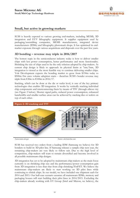
Stacking, which can be done at the die or wafer level, is one of the key primary<br />
technologies that enables 3D integration. It works by vertically stacking individual<br />
chip components and interconnecting them by means of TSV (through-silicon via)<br />
(see Figure 2 below). Shorter signal paths, reduced power consumption, enhanced<br />
bandwidths and smaller surface areas can be achieved by stacking dies or wafers on<br />
top of each other.<br />
Figure 2: 3D stacking and TSV<br />
Source:www.nist.gov<br />
Source: electronicsbus.com<br />
SUSS has received two orders from a leading IDM (Samsung we believe) for 3D<br />
bonders to build its 3D pilot line. If Samsung releases a sample chip next year, the<br />
remaining chip-makers are very likely to follow suit. Due to the high level of<br />
competition, chip-makers will want to remain diversified and become involved in<br />
all possible mainstream chip designs.<br />
3D integration has yet to be adopted by mainstream chip-makers as the main focus<br />
currently is on shrinking chip size and the performance/power consumption gain<br />
from 3D integration is less than that from chip shrinking/FinFET. We believe the<br />
mainstream chip-makers are likely to start working on 3D pilot lines while<br />
continuing to shrink chips. In our model, we have included one shipment each for<br />
2014 and 2015. Our bull-case scenario assumes all mainstream IDMs, memory and<br />
packaging houses will start building their pilot lines in 2014/2015. Excluding the<br />
chip-makers already working with EV Group (Intel and Micron, we believe), the<br />
77