- Page 2 and 3:
MEMORY PRODUCTSDATABOOK1st EDITIONJ
- Page 4:
TABLE OF CONTENTSGENERAL INDEX Page
- Page 7 and 8:
GENERAL INDEXPageROM DEVICES ......
- Page 10 and 11:
GENERAL INFORMATIONThe SGS-THOMSON
- Page 12 and 13:
SELECTION GUIDECMOS UV EPROMPart Nu
- Page 14 and 15:
SELECTION GUIDECMOS OTP ROMPart Num
- Page 16 and 17:
SELECTION GUIDEZEROPOWERPart Number
- Page 18 and 19:
SELECTION GUIDEFAST STATIC RAMPart
- Page 20 and 21:
12 32Kx8 NMOS M27256FUV EPROMPRODUC
- Page 22 and 23:
VFSRAMPRODUCTDESCRIPTIONSGS-THOMSON
- Page 24:
EPROM DEVICESNMOS UV EPROM23
- Page 27 and 28:
ET2716/M2716BLOCK DIAGRAM~ VPP'5V+-
- Page 29 and 30:
ET2716/M2716AC TEST CONDITIONSOutpu
- Page 31 and 32:
ET2716/M2716ERASINGThe M/ET2716 is
- Page 33 and 34:
ET2716/M2716SWITCHING TIME WAVEFORM
- Page 36 and 37:
M2732A32K (4K x 8) NMOS UV ERASABLE
- Page 38 and 39:
M2732AREAD OPERATIONDC AND AC CONDI
- Page 40 and 41:
M2732APROGRAMMING OPERATION(l) (T a
- Page 42:
M2732APROGRAMMING OPERATION (Contin
- Page 45 and 46:
M2764ABLOCK DIAGRAMDATA OUTPUT00- 0
- Page 47 and 48:
M2764AREAD OPERATION (Continued)AC
- Page 49 and 50:
M2764ADEVICE OPERATION (Continued)T
- Page 51 and 52:
M2764APROGRAMMING WAVEFORMSV1HADDRE
- Page 53 and 54:
M2764AORDERING INFORMATIONPart Numb
- Page 55 and 56:
M27128ABLOCK DIAGRAMVceO--GND o--
- Page 57 and 58:
M27128AREAD OPERATION (Continued)AC
- Page 59 and 60:
M27128ADEVICE OPERATION (Continued)
- Page 61 and 62:
M27128APROGRAMMING WAVEFORMSIVIHADD
- Page 63 and 64:
M27128AORDI:RING INFORMATIONPart Nu
- Page 65 and 66:
M27256BLOCK DIAGRAMVeco----GNOo-
- Page 67 and 68:
M27256READ OPERATION (Continued)AC
- Page 69 and 70:
M27256DEVICE OPERATION (Continued)P
- Page 71 and 72:
M27256PROGRAMMING WAVEFORMSPROGRAMP
- Page 73 and 74:
M27256ORDERING INFORMATIONPart Numb
- Page 75 and 76:
M27512BLOCK DIAGRAMVee o-----?GNOO-
- Page 77 and 78:
M27512AC TEST CONDITIONSOutput Load
- Page 79 and 80:
M27512DEVICE OPERATIONS (Continued)
- Page 81 and 82:
M27512DEVICE OPERATION (Continued)M
- Page 83 and 84:
M27512PROGRAMMING OPERATION (T amb=
- Page 85 and 86:
M27512M27512 DESIGN INNOVATIONS FOR
- Page 87 and 88:
M27512Figure 7 - M27512 Sensing sch
- Page 90:
EPROM DEVICESCMOS UV EPROM89
- Page 93 and 94:
ETC2716BLOCK DIAG~AM+-- vpp+-- vcc+
- Page 95 and 96:
ETC2716AC TEST CONDITIONSOutput Loa
- Page 97 and 98:
ETC2716ERASING~he ETC?716 !s erased
- Page 99 and 100:
ETC2716SWITCHING TIME WAVEFORMSR.ed
- Page 102 and 103:
ETC273232K BIT (4K x 8) CMOS UV ERA
- Page 104 and 105:
ETC2732READ OPERATIONDC CHARACTERIS
- Page 106 and 107:
ETC2732DEVICE OPERATIONThe five mod
- Page 108 and 109:
ETC2732PROGRAMMING WAVEFOR'''SNote:
- Page 110 and 111:
ETC2732SWITCHING TIME WAVEFORMSRead
- Page 112 and 113:
TS27C64AQ64K (8K x 8) CMOS UV ERASA
- Page 114 and 115:
TS27C64AQREAD OPERATIONDC CHARACTER
- Page 116 and 117:
TS27C64AQDEVICE OPERATIONThe seven
- Page 118 and 119:
TS27C64AQAC TEST CONDITIONSInput ri
- Page 120:
TS27C64AQORDERING INFORMATIONPart N
- Page 123 and 124:
TS27C256QBLOCK DIAGRAMVee 0----.GND
- Page 125 and 126:
TS27C256QAC TEST CONDITIONSOutput L
- Page 127 and 128:
TS27C256QERASINGThe TS27C256 is era
- Page 129 and 130:
TS27C256QHIGH SPEED PROGRAMMING FLO
- Page 131 and 132:
,1,;'"
- Page 133 and 134:
ST27C1001BLOCK DIAGRAMv P P cr-----
- Page 135 and 136:
M27C1024BLOCK DIAGRAMVpp 0----:---+
- Page 137 and 138:
M27C1024AC TEST CONDITIONSOutput Lo
- Page 139 and 140:
M27C,1024PROGRAM INHIBITProgramming
- Page 141 and 142:
M27C1024PROGRAMMING WAVEFORMSVIHADD
- Page 143 and 144:
M27C1024ORDERING INFORMATIONPart Nu
- Page 146 and 147:
ST2764AP64K (8K x 8) NMOS ONE TIME
- Page 148 and 149:
ST2764APREAD OPERA nONDC AND AC CON
- Page 150 and 151:
ST2764APDEVICE OPERATIONThe seven m
- Page 152 and 153:
ST2764APPROGRAMMING OPERATION (Tamb
- Page 154 and 155:
ST2764APFAST PROGRAMMING FLOWCHART9
- Page 156 and 157:
ST27128AP128K (16K x 8) NMOS ONE TI
- Page 158 and 159:
ST27128APREAD OPERATIONDC AND AC CO
- Page 160 and 161:
ST27128APDEVICE OPERATIONThe seven
- Page 162 and 163:
ST27128APPROGRAMMING OPERATION (Tam
- Page 164 and 165:
ST27128APFAST PROGRAMMING FLOWCHART
- Page 166 and 167:
ST27256P256K (32K x 8) NMOS ONE TIM
- Page 168 and 169:
ST27256PREAD OPERATIONDC AND AC CON
- Page 170 and 171:
ST27256PDEVICE OPERATIONThe eight m
- Page 172 and 173:
ST27256PPROGRAMMING OPERATION (Tamb
- Page 174 and 175:
ST27256PFAST PROGRAMMING FLOWCHARTF
- Page 176:
EPROM DEVICESCMOS OTP ROM175
- Page 179 and 180:
TS27C64AFN-TS27C64APBLOCK DIAGRAMVe
- Page 181 and 182:
TS27C64AFN-TS27C64APAC TEST CONDITI
- Page 183 and 184:
TS27C64FN-TS27C64APPROGRAMMINGOPERA
- Page 185 and 186:
TS27C64AFN-TS27C64APHIGH SPEED PROG
- Page 187 and 188:
TS27C64AFN~TS27C64APORDERING INFORM
- Page 189 and 190:
ST27C256FN-ST27C256PBLOCK DIAGRAMVc
- Page 191 and 192:
ST27C256FN·ST27C256PAC TEST CONDIT
- Page 193 and 194:
ST27C256FN-ST27C256PPROGRAMMING CHA
- Page 195 and 196:
ST27C256FN·ST27C256PHIGH SPEED PRO
- Page 197 and 198:
ST27C256FN-ST27C256PORDERING INFORM
- Page 200 and 201:
SGS-1HOMSON~ ., L ~D©ffi1@rn[brn©
- Page 202 and 203:
M8571ELECTRICAL CHARACTERISTICS (0
- Page 204 and 205:
M8571S-BUS DESCRIPTION (Continued)A
- Page 206 and 207:
M8571S·BUS INTERFACEThe serial, 3-
- Page 208 and 209:
M8571MASTER. READS AFTER SETTING WO
- Page 210:
M8571ORDERING INFORMATIONPort Numbe
- Page 213 and 214:
M9306BLOCK DIAGRAM00DI---+-+-+-+---
- Page 215 and 216:
M93D6FUNCTIONAL DESCRIPTIONThe inpu
- Page 217 and 218:
M9306ORDERING INFORMATIONPart Numbe
- Page 219 and 220:
M9346BLOCK DIAGRAMDl~-r------------
- Page 221 and 222:
M9346FUNCTIONAL DESCRIPTIONThe inpu
- Page 223 and 224:
M9346INSTRUCTION SETInstruction S8
- Page 225 and 226:
M9346TIMING DIAGRAMS (Continued)INS
- Page 228:
EEPROM DEVICESCMOS EEPROM227
- Page 231 and 232:
ST24C02BLOCK DIAGRAMseL--~~--~-----
- Page 233 and 234:
ST24C02FIG. 2A· DATA TRANSFER SEQU
- Page 235 and 236:
ST24C02ELECTRICAL CHARACTERISTICSAC
- Page 237 and 238:
ST24C02FIG. 4A· PAGE WRITEBUS ACTI
- Page 240 and 241:
TS59C111 K BIT SERIAL CMOS EEPROM
- Page 242 and 243:
TS59C11READ OPERATIONDC CHARACTERIS
- Page 244 and 245:
TS59C11The READ instruction is the
- Page 246 and 247:
TS59C11FIG. 5b - ERAL (Erase all) M
- Page 248 and 249:
~ SGS-1HOMSONIt.. ~ L [j\I'A]O©OO@
- Page 250 and 251:
TS93C46READ OPERATIONDC CHARACTERIS
- Page 252 and 253:
TS93C46INSTRUCTION TIMINGSREADSK ~u
- Page 254:
~TS93C46ORDERING INFORMATIONPart Nu
- Page 257 and 258:
ST93C56BLOCK DIAGRAMPROTECTREGISTER
- Page 260 and 261:
M2316H16K-BIT READ ONLY MEMORY• S
- Page 262 and 263:
M2316HSTATIC ELECTRICAL CHARACTERIS
- Page 264 and 265:
M2332M233332K-BIT READ ONLY MEMORY
- Page 266 and 267:
M2332/M2333DC AND OPERATING CHARACT
- Page 268 and 269:
~ SGS-11I0MSONA., L ~D©[Ri@~[lJ~©
- Page 270 and 271:
M2364DC AND OPERATING CHARACTERISTI
- Page 272 and 273:
M236564K-BIT READ ONLY MEMORY• PI
- Page 274 and 275:
M2365DC AND OPERATING CHARACTERISTI
- Page 276:
STATIC RAM DEVICES275
- Page 279 and 280:
MK48Z02N2(B)-12115/20/25DESCRIPTION
- Page 281 and 282:
MK48Z02112(B)-12115/20/25WRITE MODE
- Page 283 and 284:
MK48Z02/12(B)-12/15/20/25FIGURE 6.
- Page 285 and 286:
MK48Z02/12(B)-12/15/20/25FIGURE 7.
- Page 287 and 288:
MK48Z02112(B}-12115/20/25AC TEST CO
- Page 290 and 291:
MK48C02A/12A(K, N)·15/20/252K x 8
- Page 292 and 293:
MK48C02AI12A(K,N)-15/20/25OPERATION
- Page 294 and 295:
MK48C02A/12A(K, N)-15/20/25DATA RET
- Page 296 and 297:
MK48C02A112A(K,N)-15/20/25FIGURE 6.
- Page 298 and 299:
MK48C02A112A(K,N)-15/20/25AC TEST C
- Page 300 and 301:
MK48T02/12(B)-12/15120/252K x 8 ZER
- Page 302 and 303:
MK48T02/12(B)-12/15/20/25OPERATIONR
- Page 304 and 305:
MK48T02N 2(8)-12/15/20/25CLOCK OPER
- Page 306 and 307:
MK48T02112(B)-12/15/20/25The FT bit
- Page 308 and 309:
MK48T02112(B)-12115/20/25PREDICTING
- Page 310 and 311:
MK48T02112(B)-12/15/20/25~redlctlng
- Page 312 and 313:
MK48TD2/12(B)-12115/20/25ABSOWTE MA
- Page 314 and 315:
M K48Z08/18/09/19(B)·15/201258K x
- Page 316 and 317:
MK48Z08/18/09/19(B)-15/20/25OPERATI
- Page 319 and 320:
MK48Z08118/09/19(B)-15/20/25AC ELEC
- Page 321 and 322:
MK48Z08118/09119(B)-15/20/25DATA RE
- Page 323 and 324:
MK48Z08118/09119(B)-15/20/25ABSOWTE
- Page 325 and 326:
MK48Z08/18/09/19(B)-15/20/25PACKAGE
- Page 327 and 328:
MKI48Z02112(B)-15/20/25DESCRIPTIONT
- Page 329 and 330:
M KI48Z02112(B)-15/20J25WRITE MODET
- Page 331 and 332:
MKI48Z02/12(B.)-15/20/25FIGURE.6. P
- Page 333 and 334: MKI48Z02/12(B)-15/20/25FIGURE 7. MK
- Page 335 and 336: MKI48Z02112(B)-1S/20/2SAC TEST COND
- Page 338 and 339: ~ SGS-THOMSON..""! L ~o©oo@rn[!J~
- Page 340 and 341: MK48T08 (8)-10/12/15/20READ MODEThe
- Page 342 and 343: MK48T08 (8)-10/12/15/20AC ELECTRICA
- Page 344 and 345: MK48T08 (8)-10/12/15/20CLOCK OPERAT
- Page 346 and 347: MK48T08 (B)-10112/15/20FIGURE 8. FR
- Page 348 and 349: MK48T08 (8)-10/12/15/20rhe t 10/0 f
- Page 350: MK48T08 (8)-10/12/15/20PACKAGE DESC
- Page 354: STATIC RAM DEVICESCACHE TAG RAM353
- Page 357 and 358: MK41 HSO(N, P)-20/25/35FIGURE 2. CO
- Page 359 and 360: MK41H80(N,P)-20/25/35APPLICATIONThe
- Page 361 and 362: MK41H80(N,P)-20/25/35ABSOWTE MAXIMU
- Page 363 and 364: MK41 H80(N ,P)-20/25/35NORMALIZED D
- Page 365 and 366: MK41H8O(N,P),-2OI2513522 PIN "P" PA
- Page 367 and 368: MK4202(Q)-20TRUTH TABLERS S E WHi -
- Page 369 and 370: MK4202(Q)-20DEVICE DESCRIPTION AND
- Page 371 and 372: MK4202(Q)-20READ MODEThe MK4202 is
- Page 373 and 374: MK4202(Q)-20COMPARE CYCLE TIMINGEle
- Page 375 and 376: MK4202(Q)-20FIGURE 5. W WRITE CYCLE
- Page 377 and 378: MK4202(Q)-20FIGURE 10. CHIP SELECT
- Page 379 and 380: MK4202(Q)-20FIGURE 15. LATE WRITE·
- Page 381 and 382: MK4202(Q)-20FIGURE 21. RESET CYCLEr
- Page 383: MK4202(Q)-20AC TEST CONDITIONSInput
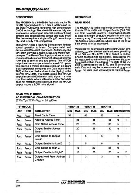
- Page 387 and 388: MK48H74(N,P,E)-35/45/55WRITE MODETh
- Page 389 and 390: MK48H74(N, P, E)-35/45/S5COMPARE MO
- Page 391 and 392: MK48H74(N,P,E)-35/45/55APPLICATIONT
- Page 393 and 394: MK48H74(N,P,E)-35/45/55AC TEST COND
- Page 396: STATIC RAM DEVICESFIFO395
- Page 399 and 400: MK4501(N,K)-65/80/10112115/20a rate
- Page 401 and 402: MK4501 (N, K)-65/80/1 0112/15/20REA
- Page 403 and 404: MK4501 (N, K)-65/80/10/12/15/20RESE
- Page 405 and 406: M K4501(N, K)-65/80110/12115/20SING
- Page 407 and 408: MK4501(N,K)-65/80110112/15/20EXPANS
- Page 409 and 410: MK4501(N, K)-65/80110/12/15/20COMPO
- Page 411 and 412: MK4501 (N, K)-65/80110112115/20FIGU
- Page 414 and 415: ~ SGS-1HOMSON,."'! I. ~u©oo@rn[brn
- Page 416 and 417: MK4503(N,K)-50/65/80/10/12/15/20WRI
- Page 418 and 419: MK4S03(N ,K)-SO/6S/80/1 0/12/1S/20F
- Page 420 and 421: MK4503(N ,K)-50/65/80110112/15/20RE
- Page 422 and 423: MK4S03(N, K)-S0/6S/80110112/1S/20HA
- Page 424 and 425: MK4S03(N ,K)-SO/6S/80110112I1S/20EX
- Page 426 and 427: MK4503(N, K)-50/65/80/10112/15/20CO
- Page 428 and 429: MK4S03(N, K)-SO/6S/80/1 0/1211 S/20
- Page 430 and 431: MK4511(N,K)-12/15/20512 x 8 CMOS Bi
- Page 432 and 433: MK4511(N,K)-12115/20READ MODEThe MK
- Page 434 and 435:
MK4511(N,K)-12115/20DUAL PORT OPERA
- Page 436 and 437:
MK4511 (N,K)-12115/20IMPLEMENTATION
- Page 438 and 439:
MK4511(N,K)-12/15/20ABSOWTE MAXIMUM
- Page 440:
MK4511(N,K)-12115/20FIGURE 11. MK45
- Page 443 and 444:
M K4505M/4505S(N)-25/33/50DESCRIPTI
- Page 445 and 446:
MK4505M/4505S(N)-25/33/50AC ELECTRI
- Page 447 and 448:
MK4505M/4505S(N)-25/33/50FIGURE S.
- Page 449 and 450:
M K4505M/4505S(N)-25/33/50FIGURE 9.
- Page 451 and 452:
MK4505M/4505S(N)-25/33/50SIMULTANEO
- Page 453 and 454:
MK4505M/4505S{N)-25/33/50FIGURE 13.
- Page 455 and 456:
MK4505M/4505S(N)-25/33/50ABSOWTE MA
- Page 457 and 458:
MK4S0SM/4S0SS(N)-2S/33/S020 PIN uN"
- Page 459 and 460:
MK4S264/4S26S(N)-SS/70FIGURE 2. DEV
- Page 461 and 462:
MK45264/45265(N)-55nOAC ELECTRICAL
- Page 463 and 464:
MK45264/45265(N)-55noReadlWriteThe
- Page 465 and 466:
MK45264/45265(N)-55noFIGURE 8. FULL
- Page 467 and 468:
MK4S264/4S26S(N)-SSnoFIGURE 13. TRA
- Page 469 and 470:
MK45264/45265(N)-55noFIGURE 18. WRI
- Page 471 and 472:
MK4S264/4S26S(N)-SSI7OAC TEST CONDI
- Page 473 and 474:
MK45264/45265(~)-5snoWidth Expansio
- Page 475 and 476:
MK45264/45265(N)-55noORDERING INFOR
- Page 478 and 479:
MK41H661M K41 H67(N, P)-20/25/3516K
- Page 480 and 481:
MK41H66/MK41 H67(N, P)-20/25/35WRIT
- Page 482 and 483:
MK41H66/MK41H67(N,P)-20/25135APPLIC
- Page 484 and 485:
MK41H66/MK41H67{N,P)-20/25/35NORMAL
- Page 486 and 487:
MK41 H66/MK41 H67(N ,P)-20/25/35ORD
- Page 488 and 489:
MK41H681MK41H69(N,P)-20/25/354K x 4
- Page 490 and 491:
MK41 H68/MK41 H69(N, P)-20/25/35WRI
- Page 492 and 493:
MK41H68/MK41 H69(N ,P)-20/25/35APPL
- Page 494 and 495:
MK41 H68/MK41 H69(N ,P)-20/25/35NOR
- Page 496 and 497:
MK41H68/MK41H69(N,P)-20/25/35ORDERI
- Page 498 and 499:
t==' SGS-1HOMSON. ..,1. ~o©oo@rn[]
- Page 500 and 501:
MK41 H79(N,P)·20125/35WRITE MODETh
- Page 502 and 503:
MK41 H79(N, P)-20/25/35ITANDBY MODE
- Page 504 and 505:
MK41 H79(N ,P)-20/25/35"C TEST COND
- Page 506 and 507:
MK41H79(N,P)-20/25/35~ORMALIZED DC
- Page 508 and 509:
MK41 H87(N)-25/35/4564K x 1 CMOS ST
- Page 510 and 511:
MK41H87(N)-25/35/45WRITE MODEThe MK
- Page 512 and 513:
MK41H87(N)-25/35/45STANDBY MODEThe
- Page 514 and 515:
MK41 H87(N)-25/35/45AC TEST CONDITI
- Page 516 and 517:
.35, 45, 55, AND 70 ns ADDRESS ACCE
- Page 518 and 519:
MK48H64/MK48H65(N,P)-35/45/55noREAD
- Page 520 and 521:
MK48H64/MK48H65(N,P)-35/45/55noWRIT
- Page 522 and 523:
MK48H64/MK48H65(N,P)-35/45/55noABSO
- Page 524:
SALES OFFICESAUSTRALIANSW 2027 EDGE
- Page 527:
Information furnished is believed t