Ion Implantation and Synthesis of Materials - Studium
Ion Implantation and Synthesis of Materials - Studium
Ion Implantation and Synthesis of Materials - Studium

You also want an ePaper? Increase the reach of your titles
YUMPU automatically turns print PDFs into web optimized ePapers that Google loves.
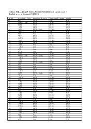
14.4 Issues <strong>of</strong> <strong>Ion</strong> <strong>Implantation</strong>s During Device Scaling 20714.3.6 Gate ImplantAt the same time as source/drain implantation, the polycrystalline silicon gates aresimultaneously doped by ion implantation. After the source/drain/gate doping, arapid thermal anneal is required to activate the dopants <strong>and</strong> repair lattice damagescreated by the implantation. Different from diffusion in monocrystalline bulksilicon, dopant diffusion in the polycrystalline silicon gate material is very fast.This is due to the grain boundaries in polycrystalline silicon, which providedopants with quick diffusion pathways (Wolf <strong>and</strong> Tauber 1986). This rapiddiffusion <strong>of</strong> dopants results in a more uniform doping distribution at shortannealing times. Phosphorus, boron, <strong>and</strong> arsenic are usually used for gate doping.It is critical that the dopants do not diffuse into the channel region. The presence<strong>of</strong> a thin oxide layer between the polycrystalline silicon gate <strong>and</strong> the substrate issufficient to block most <strong>of</strong> the diffusion. However, if some <strong>of</strong> gate dopantspenetrate through the oxide layer, an undesired threshold voltage variation willoccur (Schaber 1985).Dopant penetration can be a serious issue for alternative high-permittivity (highk)gate dielectric materials. One typical example is HfO 2 . It has been reported thatthe dopant penetration through HfO 2 is accelerated by the presence <strong>of</strong> grainboundaries that form when an amorphous HfO 2 layer is transformed into apolycrystalline layer after high temperature annealing (Quevedo-Lopez et al.2002). To reduce dopant penetration, several different approaches have beenproposed, which include either incorporating other impurities into the dielectriclayer or by depositing a thin intermediate buffer layer between the polycrystallinesilicon gate <strong>and</strong> the gate dielectric layer (Park et al. 2000).14.4 Issues <strong>of</strong> <strong>Ion</strong> <strong>Implantation</strong>s During Device ScalingShrinking devices dem<strong>and</strong> a higher level <strong>of</strong> control <strong>of</strong> the ion implantation dose<strong>and</strong> ion energy purity. Extreme low energy ion beams with high beam currents are<strong>of</strong> crucial importance to achieve the production needs <strong>of</strong> CMOS devices withphysical gate lengths less than 100 nm. Both conditions require the production <strong>of</strong>new implant tools that can minimize space charge effects, energy contamination,<strong>and</strong> beam shadowing effects.14.4.1 Space Charge EffectsDuring ion beam transport along the beam line, the beam will experience a blowupas a consequence <strong>of</strong> the mutual repulsion <strong>of</strong> the charged particles. Themagnitude <strong>of</strong> this space-charge phenomenon is related to the charge-state, Z, thebeam energy, E, <strong>and</strong> the mass <strong>of</strong> particles, m. The space charge effect can beapproximated by Kanaya et al. (1972)