

Online proceedings - EDA Publishing Association
Online proceedings - EDA Publishing Association
Online proceedings - EDA Publishing Association

Create successful ePaper yourself
Turn your PDF publications into a flip-book with our unique Google optimized e-Paper software.
7-9 October 2009, Leuven, Belgium<br />
of the silicon bench can greatly reduce package size and<br />
interconnection length within components, which result in<br />
reduction of parasitic capacitance and inductance in the<br />
package suitable for high-speed applications. Meanwhile, the<br />
SiOB provides exclusive advantages of high precisely optical<br />
alignment for low insertion loss coupling from optical<br />
components to fiber core, good thermal mismatch, excellent<br />
thermal conductivity, and better resistor fabrication for<br />
impedance matching of signal transmission. On the other<br />
hand, SiOB still has its intrinsic shortcoming. Silicon<br />
substrate is lossy material in the RF/microwave/millimeter<br />
wave regimes. Electrical signals transmitted between on-chip<br />
circuitries can easily leak into silicon substrate and be coupled<br />
to generate substrate noise. Electrical losses of the signals<br />
due to induced eddy current in the substrate also degrade the<br />
quality of the performance of passive components in the<br />
driving circuitry. In order to resolve this issue, a layer of 3µm<br />
BCB (benzo-cyclo-butene) is utilized for passive fabrication<br />
where the loss can be greatly reduced. Owing to high thermal<br />
resistance characteristic of BCB, laser diode directly mounted<br />
on the top of it would have inevitable working temperature<br />
raise that could affect the laser performance.<br />
Therefore, in this paper, the equivalent ETCM of SiOB<br />
mounted with 160Gbp/s VCSELs will be developed by<br />
considering the characteristics of device materials and<br />
geometries. The presented model can not only reasonably<br />
simplify the complicated configuration but also provide an<br />
indication for system optimization.<br />
II.<br />
MODEL ANALYSIS<br />
According to the essential meanings and emphases of<br />
common π-circuit model, three main blocks, labeled heating<br />
source, propagated resistance, and common base resistance,<br />
are employed in the general electrothermal network π-model,<br />
shown in Fig. 1, representing the thermal source, thermal flow<br />
path, and the common base of thermal conducting system,<br />
respectively. As mentioned by A. M. Darwish et al. that it is<br />
appropriate to assign adiabatic surface between each heating<br />
source and the next [2], the adopted dash-lines in the network<br />
π-model represent an adiabatic surface enclosed each<br />
presented blocks where the effective contact area can be<br />
eventually well defined. Meanwhile, the impedance<br />
parameters Z i , where i present 1, 2, 3, and 4, can be defined as<br />
the thermal resistance of heating source itself, source-source,<br />
nature or forced air convection, thermal capacitance, and<br />
other specified boundary conditions, and so on. Boundary A<br />
and B can be the ground level of the thermal flows, other<br />
heating components of thermal conducting system with<br />
specified thermal conditions, or interconnections between<br />
different systems. It should be specially emphasized that<br />
icons of the source of thermal flow and the block of heating<br />
source represent the thermal generation and flow and main<br />
heated component, respectively.<br />
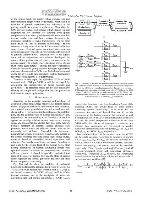
Fig. 3(a) and (b) show the modified electrothermal<br />
π-network model and the associated equivalent ETCM of the<br />
VCSELs on SiOB, respectively, where Z 1 and Z 2 , Z 3 , and Z 4<br />
are thermal resistance of a VCSEL (R VCSEL ) itself, an infinite<br />
thermal resistance due to the negligence of nature air<br />
convention here, and thermal capacitance of SiOB (C SiOB ),<br />
respectively. Boundary A and B are the adjacent R VCSEL of the<br />
operating VCSEL and ground level for entire thermal<br />
conducting system, respectively. It is noted that two<br />
parameters, the source of thermal flow and Z 1 , are the<br />
components of the heating source in the modified network<br />
π-model since the VCSELs are main thermal flow generators<br />
and also the heated components themselves in our case.<br />
Additionally, the blocks of propagated resistances and<br />
common base resistances are represented by parallel<br />
connection of thermal resistance of gold (R Gold ), air (R Air ), and<br />
BCB (R BCB ) and SiOB (R SiOB ), respectively.<br />
Four switches adopted in the structure mean the VCSEL<br />
can be single operated. According to Fourier’s conduction<br />
law, R VCSEL , R Gold , R Air , and R BCB can be easily calculated as R i<br />
=t i /k i A i , where i, t, k, and A are adopted material, thickness,<br />
thermal conductivity, and contact area of the materials,<br />
respectively. Then, C SiOB is equal to Q/∆T where Q and ∆T<br />
represent dissipated power and temperature difference,<br />
respectively. Parameter R SiOB , however, has complicated<br />
thermal behavior due to its large volume and aspect ratio. It<br />
can be calculated as follows [2]:<br />
[ f ( g[ 2s]<br />
1)<br />
]<br />
1 ⎛ V + ⎞ 1 ⎛ h( 2.<br />
3t)<br />
⎞<br />
R SiOB<br />
= ln⎜<br />
+ ⎜ ⎟<br />
[ ( [ ])] ⎟<br />
ln , (1)<br />
2π Wk ⎝ V f g L ⎠ 4π sk ⎝ h(s) ⎠<br />
where<br />
(a)<br />
(b)<br />
Fig. 3. (a)Scheme of the modified general electrothermal network π-model.<br />
The source of thermal flow and Z 1 are the components of the heating source<br />
due to the VCSELs are main heating generators themselves in our case.<br />
(b)The equivalent electrothermal circuit model of the VCSELs on the SiOB,<br />
where Z 1 and Z 2, Z 3, and Z 4 are thermal resistance of VCSEL (R VCSEL), an<br />
infinite thermal resistance due to without nature air convention here, and<br />
thermal capacitance of SiOB (C SiOB), respectively.<br />
©<strong>EDA</strong> <strong>Publishing</strong>/THERMINIC 2009 9<br />
ISBN: 978-2-35500-010-2


