

Online proceedings - EDA Publishing Association
Online proceedings - EDA Publishing Association
Online proceedings - EDA Publishing Association

Create successful ePaper yourself
Turn your PDF publications into a flip-book with our unique Google optimized e-Paper software.
III.<br />
CASE STUDY: 2 STACKED DIE STRUCTURE<br />
In this the section the general approach detailed thermal<br />
modeling presented in the previous section for is applied on<br />
specific 3D integrated structure. A schematic of the test case<br />
is shown in Fig.3. The test case consists of a two die stacked<br />
structure in a BGA package. The BGA package in soldered<br />
to a PBC and the whole structure considered to be in an<br />
ambient environment of still air at 300K. The top die is a 25<br />
µm thick die, 5x5 mm² in size. The active region of the top<br />
die is connected to the bottom die by means of Cu through-<br />
Si vias (TSVs) through the top die [13]. These vias have a<br />
diameter of 5µm. Several pitches of the TSVs are considered<br />
to study the effect of the TSV on the thermal behavior or the<br />
stack. The bottom die is an 8x8 mm² die with a thickness of<br />
250µm. The different steps of the procedure presented in<br />
Fig. 2 with now be dealt with in detail.<br />
A. Definition of simulation domain<br />
First the region of interest is selected in the structure. In<br />
this domain the detailed numerical simulation will be<br />
performed. In this test case the stack including the 2 Si dies,<br />
the adhesive layer in between the dies. Also all the<br />
interconnections between the two dies and the complete back<br />
end of line structure (BEOL) of both dies are included in the<br />
model. To simplify the geometry of the simulation domain<br />
part of the overmold compound surrounding the top die is<br />
included in the model.<br />
B. Package model<br />
The region outside the simulation domain is converted to<br />
thermal boundaries conditions applied on the simulation<br />
domain. Inside FireBolt, the boundary conditions are<br />
formulated for each face S i with uniform heat transfer<br />
coefficient h i and thermal capacitance c i parameters as<br />
shown in the following equation where φ is the flux density:<br />
dT ( ri<br />
)<br />
ϕ r = h ⋅ T r − T + c ⋅ with r ∈S<br />
(2)<br />
( ) ( ( ) )<br />
i i i A i i i<br />
dt<br />
Here the parameters of the package model are extracted<br />
from a full 3D finite element model of the package and PCB.<br />
For the finite element analysis the software tool Msc.Marc is<br />
used. From this thermal model the heat flow through each of<br />
the faces of the simulation domain can be obtained and<br />
converted to boundary conditions in the form of RC thermal<br />
networks, to be used in the detailed model.<br />
7-9 October 2009, Leuven, Belgium<br />
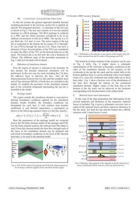
Bottom view<br />
Heat flux (W/mm 2 )<br />
Fig. 5. Distribution of the heat flux at one quarter of the bottom of the die<br />
stack extracted from the FE model of the package and PCB.<br />
The board level finite element of the structure can be seen<br />
in Fig. 4 (left). Fig. 4 (right) shows a schematic<br />
representation of RC networks as boundary conditions at the<br />
sides of the simulation domain. At the location of the<br />
wirebonds at the top the die stack and the solder balls at the<br />
bottom addition faces S i can be attributed with a local higher<br />
value of h i , since the wirebonds and solder balls act as local<br />
heat sinks. Fig. 5 show a bottom view of the distribution of<br />
the heat flow through the bottom of the considered<br />
simulation domain. Higher values of the heat flux at the<br />
bottom of the die stack can be observed at the locations<br />
corresponding with the placement of the solders balls.<br />
C. Material layer stack information<br />
In this step of the data preparation the information of the<br />
several materials and thickness of the respective material<br />
layers is included. Fig. 6 gives a schematic overview (not to<br />
scale) of the material layers and their respective thickness in<br />
the die stack. For both the top and the bottom die a BEOL<br />
structure with 2 metal layers is used.<br />
PASSIV_T<br />
METAL2_T<br />
METAL1_T<br />
CA_T<br />
BULK_T<br />
TSV<br />
bump<br />
metal<br />
metal<br />
via<br />
250nm<br />
poly 150nm<br />
500 nm SiN<br />
330nm Si0 2<br />
600nm Si0 2<br />
500nm Si0 2<br />
300nm Si0 2<br />
400nm Si0 2<br />
25 um Si<br />
50 nm SiC<br />
50 nm SiC<br />
50 nm SiC<br />
50 nm SiC<br />
50 nm SiN<br />
METAL2_B<br />
metal<br />
600nm Si0 2<br />
50 nm SiC<br />
via<br />
500nm Si0 2<br />
50 nm SiC<br />
METAL1_B<br />
metal<br />
300nm Si0 2<br />
50 nm SiC<br />
CA_B<br />
BULK_B<br />
250nm<br />
poly 150nm<br />
400nm Si0 2<br />
250um Si<br />
50 nm SiN<br />
Fig. 4. Full 3D FE model of the package and PCB (left). Representation of<br />
the boundary conditions applied on the simulation domain (right).<br />
Fig. 6. Schematic representation of the materials in the die stack (not to<br />
scale), including the BEOL structure of the top and bottom die.<br />
©<strong>EDA</strong> <strong>Publishing</strong>/THERMINIC 2009 47<br />
ISBN: 978-2-35500-010-2


