

Online proceedings - EDA Publishing Association
Online proceedings - EDA Publishing Association
Online proceedings - EDA Publishing Association

You also want an ePaper? Increase the reach of your titles
YUMPU automatically turns print PDFs into web optimized ePapers that Google loves.
impact on the mechanical stress within and in between the<br />
various compounds of the packaged die.<br />
Figure 3 shows the resulting temperature map, with a<br />
maximum temperature of 125 0 C in the right upper corner<br />
and a maximum temperature gradient of 23 0 C<br />
7-9 October 2009, Leuven, Belgium<br />
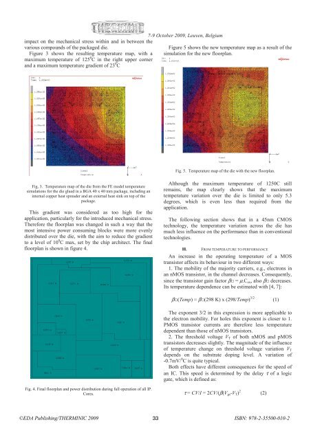
Figure 5 shows the new temperature map as a result of the<br />
simulation for the new floorplan.<br />
Fig. 5. Temperature map of the die with the new floorplan.<br />
Fig, 3. Temperature map of the die from the FE model temperature<br />
simulations for the die glued in a BGA 40 x 40 mm package, including an<br />
internal copper heat spreader and an external heat sink on top of the<br />
package.<br />
This gradient was considered as too high for the<br />
application, particularly for the introduced mechanical stress.<br />
Therefore the floorplan was changed in such a way that the<br />
most intensive power consuming blocks were more evenly<br />
distributed over the die, with the aim to reduce the gradient<br />
to a level of 10 0 C max, set by the chip architect. The final<br />
floorplan is shown in figure 4.<br />
Although the maximum temperature of 1250C still<br />
remains, the map clearly shows that the maximum<br />
temperature variation over the die is limited to only 5.3<br />
degrees, which is even less than required from the<br />
application.<br />
The following section shows that in a 45nm CMOS<br />
technology, the temperature variation across the die has<br />
much less influence on the performance than in conventional<br />
technologies.<br />
III. FROM TEMPERATURE TO PERFORMANCE<br />
An increase in the operating temperature of a MOS<br />
transistor affects its behaviour in two different ways:<br />
1. The mobility of the majority carriers, e.g., electrons in<br />
an nMOS transistor, in the channel decreases. Consequently,<br />
since the transistor gain factor β□ = μ.C ox , also β□ decreases.<br />
Its temperature dependence can be estimated with [4, 7]:<br />
β□(Temp) = β□(298 K) x (298/Temp) 3/2 (1)<br />
The exponent 3/2 in this expression is more applicable to<br />
the electron mobility. For holes this exponent is closer to 1.<br />
PMOS transistor currents are therefore less temperature<br />
dependent than those of nMOS transistors.<br />
2. The threshold voltage V T of both nMOS and pMOS<br />
transistors decreases slightly. The magnitude of the influence<br />
of temperature change on threshold voltage variation V T<br />
depends on the substrate doping level. A variation of<br />
-0.7mV/ 0 C is quite typical.<br />
Both effects have different consequences for the speed of<br />
an IC. This speed is determined by the delay τ of a logic<br />
gate, which is defined as:<br />
Fig. 4. Final floorplan and power distribution during full operation of all IP.<br />
Cores.<br />
τ = CV/I = 2CV/(β(V gs -V T ) 2 (2)<br />
©<strong>EDA</strong> <strong>Publishing</strong>/THERMINIC 2009 33<br />
ISBN: 978-2-35500-010-2


