

Online proceedings - EDA Publishing Association
Online proceedings - EDA Publishing Association
Online proceedings - EDA Publishing Association

You also want an ePaper? Increase the reach of your titles
YUMPU automatically turns print PDFs into web optimized ePapers that Google loves.
7-9 October 2009, Leuven, Belgium<br />
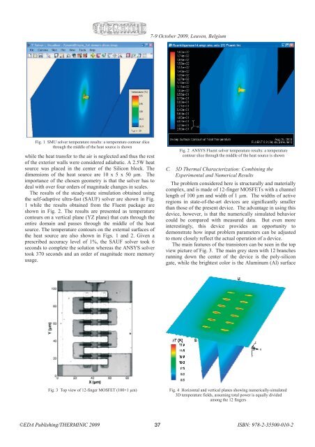
Fig. 1 SMU solver temperature results: a temperature contour slice<br />
through the middle of the heat source is shown<br />
while the heat transfer to the air is neglected and thus the rest<br />
of the exterior walls were considered adiabatic. A 2.5W heat<br />
source was placed in the center of the Silicon block. The<br />
dimensions of the heat source are 10 x 5 x 50 µm. The<br />
importance of the chosen geometry is that the solver has to<br />
deal with over four orders of magnitude changes in scales.<br />
The results of the steady-state simulation obtained using<br />
the self-adaptive ultra-fast (SAUF) solver<br />
are shown in Fig.<br />
1 while the results obtained from the Fluent package are<br />
shown in Fig. 2. The results are presented as temperature<br />
contours on a vertical plane (YZ plane) that cuts through the<br />
entire domain and passes through the middle of the heat<br />
source. The temperature contours on the external surfaces of<br />
the heat source are also shown in Figs. 1 and 2. Given a<br />
prescribed accuracy level of 1%, the SAUF solver took 6<br />
seconds to complete the solution whereas the ANSYS solver<br />
took 370 seconds and an order of magnitude more memory<br />
usage.<br />
Fig. 2 ANSYS Fluent solver<br />
temperature results: a temperature<br />
contour slice through the middle of the heat source is shown<br />
C. 3D Thermal Characterization: Combining the<br />
Experimental and Numerical Results<br />
The problem considered here is structurally and materially<br />
complex, and is made of 12-finger MOSFETs with a channel<br />
length of 100 µm and width of 1 µm. The widths of active<br />
regions in state-of-the-art devices are significantly smaller<br />
than those of the present device. The advantage in using this<br />
device, however, is that the numerically simulated behavior<br />
could be compared with measured data. But even more<br />
interestingly, this device provides an opportunity to<br />
demonstrate how input problem parameters can be adjusted<br />
to more closely reflect the actual operation of a device.<br />
The main features of the transistors can be seen in the top<br />
view picture of Fig. 3. The main grey stem with 12 branches<br />
running down the center of<br />
the device is the poly-silicon<br />
gate, while the brightest color is the Aluminum (Al) surface<br />
Fig. 3 Top view of 12-finger MOSFET<br />
(100×1 µm)<br />
Fig. 4 Horizontal and vertical planes showing numerically-simulated<br />
3D temperature fields, assuming total power is equally divided<br />
among the<br />
12 fingers<br />
©<strong>EDA</strong> <strong>Publishing</strong>/THERMINIC 2009 37<br />
ISBN: 978-2-35500-010-2


