

Superconducting Technology Assessment - nitrd
Superconducting Technology Assessment - nitrd
Superconducting Technology Assessment - nitrd

Create successful ePaper yourself
Turn your PDF publications into a flip-book with our unique Google optimized e-Paper software.
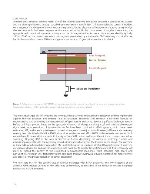
SMT MRAM<br />
Another direct selection scheme makes use of the recently observed interaction between a spin-polarized current<br />
and the bit magnetization, through so-called spin-momentum transfer (SMT). If a spin-polarized current is incident<br />
on a magnetic bit, the spin of the current-carrying spin-polarized electrons will experience a torque trying to align<br />
the electrons with their new magnetic environment inside the bit. By conservation of angular momentum, the<br />
spin-polarized current will also exert a torque on the bit magnetization. Above a critical current density, typically<br />
10 7 to 10 8 A/cm 2 , the current can switch the magnetic polarization by spin-transfer. SMT switching is most effective<br />
for bit diameters less than ~ 300 nm and gains importance as IC geometries continue to shrink.<br />
Figure 2. Schematic of a proposed SMT MRAM cell structure showing the common current path for sense and program operations.<br />
Successful development of this architecture would result in a high-density, low power MRAM.<br />
The main advantages of SMT switching are lower switching currents, improved write selectivity, and bits highly stable<br />
against thermal agitation and external field disturbances. However, SMT research is currently focused on<br />
understanding and controlling the fundamentals of spin-transfer switching. Several significant challenges remain<br />
before defining a product based on this approach. One such challenge is making a cell with a reasonable output<br />
signal level, as observations of spin-transfer so far have been confined to GMR systems, which have lower<br />
resistance, MR, and operating voltages compared to magnetic tunnel junctions. However, MTJ materials have very<br />
recently been identified with MR > 100% at very low resistances, and MR > 200% with moderate resistances. Such<br />
materials could potentially improve both the signal from SMT devices and lower the minimum currents needed for<br />
switching. Ongoing R&D in this area is directed at further decreasing the minimum switching currents and<br />
establishing materials with the necessary reproducibility and reliability for the low-resistance range. The outcome<br />
of these R&D activities will determine which SMT architectures can be used and at what lithography node. If switching<br />
currents are driven low enough for a minimum-size transistor to supply the switching current, this technology will<br />
meet or exceed the density of the established semiconductor memories, while providing high speed and<br />
non-volatility. Although SMT technology is less developed than MTJ MRAM is, it has the potential for higher density<br />
and orders-of-magnitude reduction in power dissipation<br />
We note here that for the specific case of MRAM integrated with RSFQ electronics, the low resistance of the<br />
all-metal GMR devices (instead of the MTJ) may be beneficial, as described in the follow-on section Integrated<br />
MRAM and RSFQ Electronics.<br />
178<br />
DC<br />
�<br />
� �<br />
�<br />
Free Magnet<br />
Tunnel Barrier<br />
Fixed Magnet<br />
Isolation Transistor


