

Superconducting Technology Assessment - nitrd
Superconducting Technology Assessment - nitrd
Superconducting Technology Assessment - nitrd

You also want an ePaper? Increase the reach of your titles
YUMPU automatically turns print PDFs into web optimized ePapers that Google loves.
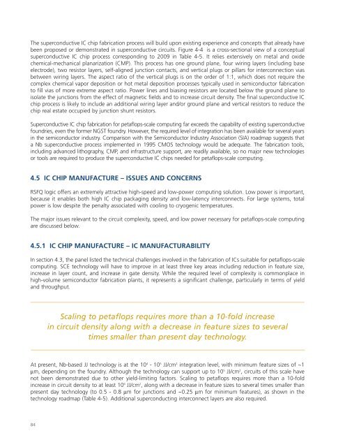
The superconductive IC chip fabrication process will build upon existing experience and concepts that already have<br />
been proposed or demonstrated in superconductive circuits. Figure 4-4 is a cross-sectional view of a conceptual<br />
superconductive IC chip process corresponding to 2009 in Table 4-5. It relies extensively on metal and oxide<br />
chemical-mechanical planarization (CMP). This process has one ground plane, four wiring layers (including base<br />
electrode), two resistor layers, self-aligned junction contacts, and vertical plugs or pillars for interconnection vias<br />
between wiring layers. The aspect ratio of the vertical plugs is on the order of 1:1, which does not require the<br />
complex chemical vapor deposition or hot metal deposition processes typically used in semiconductor fabrication<br />
to fill vias of more extreme aspect ratio. Power lines and biasing resistors are located below the ground plane to<br />
isolate the junctions from the effect of magnetic fields and to increase circuit density. The final superconductive IC<br />
chip process is likely to include an additional wiring layer and/or ground plane and vertical resistors to reduce the<br />
chip real estate occupied by junction shunt resistors.<br />
Superconductive IC chip fabrication for petaflops-scale computing far exceeds the capability of existing superconductive<br />
foundries, even the former NGST foundry. However, the required level of integration has been available for several years<br />
in the semiconductor industry. Comparison with the Semiconductor Industry Association (SIA) roadmap suggests that<br />
a Nb superconductive process implemented in 1995 CMOS technology would be adequate. The fabrication tools,<br />
including advanced lithography, CMP, and infrastructure support, are readily available, so no major new technologies<br />
or tools are required to produce the superconductive IC chips needed for petaflops-scale computing.<br />
4.5 IC CHIP MANUFACTURE – ISSUES AND CONCERNS<br />
RSFQ logic offers an extremely attractive high-speed and low-power computing solution. Low power is important,<br />
because it enables both high IC chip packaging density and low-latency interconnects. For large systems, total<br />
power is low despite the penalty associated with cooling to cryogenic temperatures.<br />
The major issues relevant to the circuit complexity, speed, and low power necessary for petaflops-scale computing<br />
are discussed below.<br />
4.5.1 IC CHIP MANUFACTURE – IC MANUFACTURABILITY<br />
In section 4.3, the panel listed the technical challenges involved in the fabrication of ICs suitable for petaflops-scale<br />
computing. SCE technology will have to improve in at least three key areas including reduction in feature size,<br />
increase in layer count, and increase in gate density. While the required level of complexity is commonplace in<br />
high-volume semiconductor fabrication plants, it represents a significant challenge, particularly in terms of yield<br />
and throughput.<br />
Scaling to petaflops requires more than a 10-fold increase<br />
in circuit density along with a decrease in feature sizes to several<br />
times smaller than present day technology.<br />
At present, Nb-based JJ technology is at the 10 4 -10 5 JJ/cm 2 integration level, with minimum feature sizes of ~1<br />
µm, depending on the foundry. Although the technology can support up to 10 5 JJ/cm 2 , circuits of this scale have<br />
not been demonstrated due to other yield-limiting factors. Scaling to petaflops requires more than a 10-fold<br />
increase in circuit density to at least 10 6 JJ/cm 2 , along with a decrease in feature sizes to several times smaller than<br />
present day technology (to 0.5 - 0.8 µm for junctions and ~0.25 µm for minimum features), as shown in the<br />
technology roadmap (Table 4-5). Additional superconducting interconnect layers are also required.<br />
84


