

Superconducting Technology Assessment - nitrd
Superconducting Technology Assessment - nitrd
Superconducting Technology Assessment - nitrd

Create successful ePaper yourself
Turn your PDF publications into a flip-book with our unique Google optimized e-Paper software.
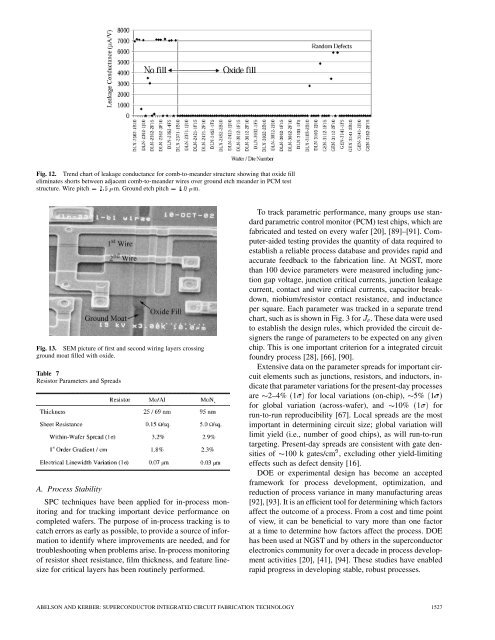
Fig. 12. Trend chart of leakage conductance for comb-to-meander structure showing that oxide fill<br />
eliminates shorts between adjacent comb-to-meander wires over ground etch meander in PCM test<br />
structure. Wire pitch aPXT "m. Ground etch pitch aRXH "m.<br />
Fig. 13. SEM picture of first and second wiring layers crossing<br />
ground moat filled with oxide.<br />
Table 7<br />
Resistor Parameters and Spreads<br />
A. Process Stability<br />
SPC techniques have been applied for in-process monitoring<br />
and for tracking important device performance on<br />
completed wafers. The purpose of in-process tracking is to<br />
catch errors as early as possible, to provide a source of information<br />
to identify where improvements are needed, and for<br />
troubleshooting when problems arise. In-process monitoring<br />
of resistor sheet resistance, film thickness, and feature linesize<br />
for critical layers has been routinely performed.<br />
To track parametric performance, many groups use standard<br />
parametric control monitor (PCM) test chips, which are<br />
fabricated and tested on every wafer [20], [89]–[91]. Computer-aided<br />
testing provides the quantity of data required to<br />
establish a reliable process database and provides rapid and<br />
accurate feedback to the fabrication line. At NGST, more<br />
than 100 device parameters were measured including junction<br />
gap voltage, junction critical currents, junction leakage<br />
current, contact and wire critical currents, capacitor breakdown,<br />
niobium/resistor contact resistance, and inductance<br />
per square. Each parameter was tracked in a separate trend<br />
chart, such as is shown in Fig. 3 for . These data were used<br />
to establish the design rules, which provided the circuit designers<br />
the range of parameters to be expected on any given<br />
chip. This is one important criterion for a integrated circuit<br />
foundry process [28], [66], [90].<br />
Extensive data on the parameter spreads for important circuit<br />
elements such as junctions, resistors, and inductors, indicate<br />
that parameter variations for the present-day processes<br />
are 2–4% 1 for local variations (on-chip), 5% 1<br />
for global variation (across-wafer), and 10% 1 for<br />
run-to-run reproducibility [67]. Local spreads are the most<br />
important in determining circuit size; global variation will<br />
limit yield (i.e., number of good chips), as will run-to-run<br />
targeting. Present-day spreads are consistent with gate densities<br />
of 100 k gates/cm , excluding other yield-limiting<br />
effects such as defect density [16].<br />
DOE or experimental design has become an accepted<br />
framework for process development, optimization, and<br />
reduction of process variance in many manufacturing areas<br />
[92], [93]. It is an efficient tool for determining which factors<br />
affect the outcome of a process. From a cost and time point<br />
of view, it can be beneficial to vary more than one factor<br />
at a time to determine how factors affect the process. DOE<br />
has been used at NGST and by others in the superconductor<br />
electronics community for over a decade in process development<br />
activities [20], [41], [94]. These studies have enabled<br />
rapid progress in developing stable, robust processes.<br />
ABELSON AND KERBER: SUPERCONDUCTOR INTEGRATED CIRCUIT FABRICATION TECHNOLOGY 1527


