

TI486 Microprocessor - Al Kossow's Bitsavers
TI486 Microprocessor - Al Kossow's Bitsavers
TI486 Microprocessor - Al Kossow's Bitsavers

You also want an ePaper? Increase the reach of your titles
YUMPU automatically turns print PDFs into web optimized ePapers that Google loves.
Overview<br />
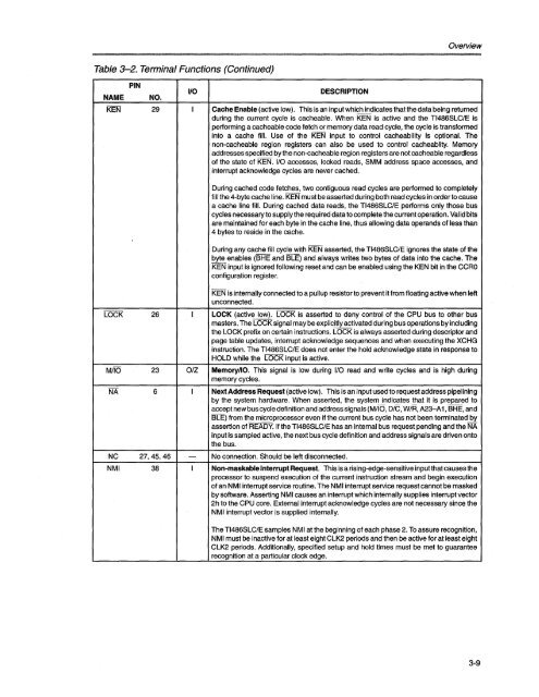
Table 3-2. Terminal Functions (Continued)<br />
NAME<br />
PIN<br />
NO.<br />
I/O<br />
DESCRIPTION<br />
KEN 29 I Cache Enable (active low). This is an input which indicates that the data being returned<br />
during the current cycle is cacheable. When KEN is active and the <strong>TI486</strong>SLC/E is<br />
performing a cacheable code fetch or memory data read cycle, the cycle is transformed<br />
into a cache fill. Use of the KEN input to control cacheability is optional. The<br />
non-cacheable region registers can also be used to control cacheablity. Memory<br />
addresses specified by the non-cacheable region registers are not cacheable regardless<br />
of the state of KEN. 1/0 accesses, locked reads, SMM address space accesses, and<br />
interrupt acknowledge cycles are never cached.<br />
During cached code fetches, two contiguous read cycles are performed to completely<br />
fill the 4-byte cache line. KEN must be asserted during both read cycles in order to cause<br />
a cache line fill. During cached data reads, the <strong>TI486</strong>SLC/E performs only those bus<br />
cycles necessary to supply the required data to complete the current operation. Valid bits<br />
are maintained for each byte in the cache line, thus allowing data operands of less than<br />
4 bytes to reside in the cache.<br />
During any cache fill cycle with KEN asserted, the <strong>TI486</strong>SLC/E ignores the state of the<br />
byte enables (BHE and BLE) and always writes two bytes of data into the cache. The<br />
KEN input is ignored following reset and can be enabled using the KEN bit in the CCRD<br />
configuration register.<br />
KEN is internally connected to a pullup resistor to prevent it from floating active when left<br />
unconnected.<br />
LOCK 26 I LOCK (active low). LOCK is asserted to deny control of the CPU bus to other bus<br />
masters. The LOCK signal may be explicitly activated during bus operations by including<br />
the LOCK prefix on certain instructions. LOCK is always asserted during descriptor and<br />
page table updates, interrupt acknowledge sequences and when executing the XCHG<br />
instruction. The <strong>TI486</strong>SLC/E does not enter the hold acknowledge state in response to<br />
HOLD while the LOCK input is active.<br />
MilO 23 OIZ MemoryllO. This signal is low during 1/0 read and write cycles and is high during<br />
memory cycles.<br />
NA 6 I Next Address Request (active low). This is an input used to request address pipelining<br />
by the system hardware. When asserted, the system indicates that it is prepared to<br />
accept new bus cycle definition and address signals (MilO, DIG, W/R, A23-A 1, BHE, and<br />
BLE) from the microprocessor even if the current bus cycle has not been terminated by<br />
assertion of READY. If the <strong>TI486</strong>SLC/E has an internal bus request pending and the NA<br />
input is sampled active, the next bus cycle definition and address signals are driven onto<br />
the bus.<br />
NC 27,45,46 - No connection. Should be left disconnected.<br />
NMI 38 I Non-maskable Interrupt Request. This is a rising-edge-sensitive input that causes the<br />
processor to suspend execution of the current instruction stream and begin execution<br />
of an NMI interrupt service routine. The NMI interrupt service request cannot be masked<br />
by software. Asserting NMI causes an interrupt which internally supplies interrupt vector<br />
2h to the CPU core. External interrupt acknowledge cycles are not necessary since the<br />
NMI interrupt vector is supplied internally.<br />
The <strong>TI486</strong>SLC/E samples NMI at the beginning of each phase 2. To assure recognition,<br />
NMI must be inactive for at least eight CLK2 periods and then be active for at least eight<br />
CLK2 periods. Additionally, specified setup and hold times must be met to guarantee<br />
recognition at a particular clock edge.<br />
3-9


