

TI486 Microprocessor - Al Kossow's Bitsavers
TI486 Microprocessor - Al Kossow's Bitsavers
TI486 Microprocessor - Al Kossow's Bitsavers

You also want an ePaper? Increase the reach of your titles
YUMPU automatically turns print PDFs into web optimized ePapers that Google loves.
Overview<br />
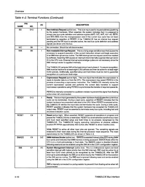
Table 4-2. Terminal Functions (Continued)<br />
NAME<br />
PIN<br />
NO.<br />
110 DESCRIPTION<br />
NA 013 I Next Address Request (active low). This is an input used to request address pipelining<br />
by the system hardware. When asserted, the system indicates that it is prepared to<br />
accept new bus cycle definition and address signals (MilO, DIG, W/R, A31-A2, BS16,<br />
and BE3-BEO) from the microprocessor even if the current bus cycle has not been<br />
terminated by assertion of READY. If the <strong>TI486</strong>DLC/E has an internal bus request<br />
pending and the NA input is sampled active, the next bus cycle definition and address<br />
signals are driven onto the bus.<br />
N/C B6 - No connection. Should be left disconnected.<br />
NMI B8 I Non-maskable Interrupt Request. This is a rising-edge-sensitive input that causes the<br />
processor to suspend execution of the current instruction stream and begin execution<br />
of an NMI interrupt service routine. The NMI interrupt service request cannot be masked<br />
by software. Asserting NMI causes an interrupt which internally supplies interrupt vector<br />
2h to the CPU core. External interrupt acknowledge cycles are not necessary since the<br />
NMI interrupt vector is supplied internally.<br />
The <strong>TI486</strong>DLC/E samples NMI at the beginning of each phase 2. To assure recognition,<br />
NMI must be inactive for at least eight CLK2 periods and then be active for at least eight<br />
CLK2 periods. Additionally, specified setup and hold times must be met to guarantee<br />
recognition at a particular clock edge.<br />
PEREa C8 I Coprocessor Request (active high). This is an input that indicates the coprocessor is<br />
ready to transfer data to or from the CPU. The coprocessor may assert PEREa in the<br />
process of executing a coprocessor instruction. The <strong>TI486</strong>DLC/E internally stores the<br />
current coprocessor opcode and performs the correct data transfers to support<br />
coprocessor operations using PEREa to synchronize the transfer of required operands.<br />
PEREa is internally connected to a pulldown resistor to prevent this signal from floating<br />
active when left unconnected.<br />
READY G13 I Ready. This is an input generated by the system hardware that indicates the current bus<br />
cycle can be terminated. During a read cycle, assertion of READY indicates that the<br />
system hardware has presented valid data to the CPU. When READY is sampled active,<br />
the <strong>TI486</strong>DLC/E latches the input data and terminates the cycle. During a write cycle,<br />
READY assertion indicates that the system hardware has accepted the <strong>TI486</strong>DLC/E<br />
output data. READY must be asserted to terminate every bus cycle, including halt and<br />
shutdown indication cycles.<br />
RESET C9 I Reset (active high). When asserted, RESET suspends all operations in progress and<br />
places the <strong>TI486</strong>DLC/E into a reset state. RESET is a level-sensitive synchronous input<br />
and must meet specified setup and hold times to be properly recognized by the<br />
<strong>TI486</strong>DLC/E. The <strong>TI486</strong>DLC/E begins executing instructions at physical address<br />
location FF FFFOh approximately 400 CLK2s after RESET is driven inactive (low).<br />
While RESET is active all other input pins are ignored. The remaining signals are<br />
initialized to their reset state during the internal processor reset sequence. The reset<br />
signal states for the <strong>TI486</strong>DLC/E are shown in Table 4-6.<br />
SMADS C6 O/Z SMM Address Strobe (active low). SMADS is asserted instead ofthe ADS during SMM<br />
bus cycles and indicates that SMM memory is being accessed. SMADS floats while the<br />
CPU is in a hold acknowledge or float state. The SMADS output is disabled (floated)<br />
following reset and can be enabled using the SMI bit in the CCR1 configuration register.<br />
SMI C7 I/O System Management Interrupt (active low). This is a bidirectional signal and level<br />
sensitive interrupt with higher priority than the NMI interrupt. SMI must be active for at<br />
least four CLK2 clock periods to be recognized by the <strong>TI486</strong>DLC/E. After the SMI<br />
interrupt is acknowledged, the SMI pin is driven low by the <strong>TI486</strong>DLC/E for the duration<br />
of the SMI service routine. The SMI input is ignored following reset and can be enabled<br />
using the SMI bit in the CCR1 configuration register.<br />
--<br />
SMI is internally connected to a pullup resistor to prevent it from floating active when left<br />
unconnected.<br />
4-10 Tl486DLCIE Bus Interface


