

TI486 Microprocessor - Al Kossow's Bitsavers
TI486 Microprocessor - Al Kossow's Bitsavers
TI486 Microprocessor - Al Kossow's Bitsavers

You also want an ePaper? Increase the reach of your titles
YUMPU automatically turns print PDFs into web optimized ePapers that Google loves.
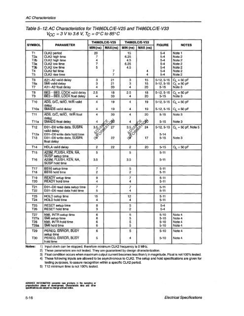
AC Characteristics<br />
Table 5-12.AC Characteristics for <strong>TI486</strong>DLCIE-V25 and <strong>TI486</strong>DLCIE-V33<br />
Vee = 3 Vto 3.6 V, Te = O°C to 85°C<br />
<strong>TI486</strong>DLC/E-V25 <strong>TI486</strong>DLC/E-V33<br />
SYMBOL PARAMETER FIGURE<br />
MIN (ns) MAX (ns) MIN (ns) MAX (ns)<br />
Notes:<br />
T1 CLK2 period 20 15 5-4<br />
T2a CLK2 high time 7 6.25 5-4<br />
T2b CLK2 high time 4 4.5 5-4<br />
T3a CLK2 low time 7 6.25 5-4<br />
T3b CLK2 low time 5 4.5 5-4<br />
T4 CLK2 fall time 7 4 5-4<br />
T5 CLK2 rise time 7 4 5-4<br />
T6 A31-A2 valid delay 3 21 3 15 5-12,5-15<br />
T6a SMI valid delay 3 21 3 15 5-12,5-15<br />
T7 A31-A2 float delay 4 30 4 20 5-15<br />
T8 BE3 - BEO, LOCK valid delay 2.5 18 2.5 18 5-12,5-15<br />
T9 BE3 - BEO, LOCK float delay 4 30 4 20 5-15<br />
T10 AOS, O/C, MilO, W/R valid 4 19 4 19 5-12,5-15<br />
~<br />
T10a SMAOS valid delay 4 19 4 19 5-12,5-15<br />
T11 AOS, O/C, MilO, W/R float 4 30 4 20 5-15<br />
~<br />
T11a SMAOS float delay 4 4 5-15<br />
T12 031-00 write data, SUSPA 3.5 27 3.5 24 5-12,5-13<br />
valid delay<br />
T12a 031-00 write data hold time 5-14<br />
T13 031-00 write data, SUSPA 22 'V 17 5-15<br />
float delay<br />
T14 HOLA valid delay 2 22 2 20 5-15<br />
T15 A20M, FLUSH, KEN, NA, 5 5 5-11<br />
SUSP setup tim~ _<br />
T16 A20M, FLUSH, KEN, NA, 3.5 3.5 5-11<br />
SUSP hold time<br />
T17 BS16 setup time 7 5 5-11<br />
T18 BS16 hold time 2 2 5-11<br />
T19 REAOY setup time 9 7 5-11<br />
T20 REAOY hold time 4 4 5-11<br />
T21 031-00 read data setup time 7 7 5-11<br />
T22 031-00 read data hold time 5 4 5-11<br />
T23 . HaLO setup time 15 12 5-11<br />
T24 HaLO hold time 4 4 5-11<br />
T25 RESET setup time 8 5 5-4<br />
T26 RESET hold time 3 2 5-4<br />
T27 NMI, INTR setup time 6 5 5-10<br />
T27a SMI setup time 6 5 5-10<br />
T28 NMI, INTR hold time 6 5 5-10<br />
T28a SMI hold time 6 5 5-10<br />
T29 PEREQ,ERROR,BUSY 6 5 5-10<br />
setuptim_e ____<br />
T30 PEREQ,ERROR,BUSY 5 4 5-10<br />
hold time<br />
Note 1<br />
Note 2<br />
Note 2<br />
Note 2<br />
Note 2<br />
Note 2<br />
Note 2<br />
NOTES<br />
CL= 50 pF<br />
CL=50 pF<br />
Note 3<br />
CL= 50 pF<br />
Note 3<br />
CL = 50 pF<br />
CL= 50 pF<br />
Note 3<br />
Note 3<br />
CL = 50 pF, Note 5<br />
Note 3<br />
CL=50pF<br />
Note 4<br />
Note 4<br />
Note 4<br />
Note 4<br />
Note 4<br />
Note 4<br />
1) Input clock can be stopped, therefore minimum CLK2 frequency is 0 MHz.<br />
2) These parameters are not tested. They are guaranteed by design characterization.<br />
3) Float condition occurs when maximum output current becomes less than II in magnitude. Float is not 100% tested.<br />
4) These following inputs are allowed to be asynchronous to CLK2. The setup and hold specifications are given for<br />
testing purposes, to assure recognition within a specific CLK2 period.<br />
5) T12 minimum time is not 100% tested.<br />
ADVANCE INFORMATION concerns new products in the sampling or<br />
preproduction phase of development. Characteristic data and other<br />
specifications are subject to change without notice.<br />
5-16 Electrical Specifications


