- Page 1 and 2:
.TEXAS INSTRUMENTS TI486 Microproce
- Page 4 and 5:
TI486 Microprocessor Reference Guid
- Page 6 and 7:
Preface Read This First About This
- Page 8 and 9:
About This Manual Appendix D Orderi
- Page 10 and 11:
Contents 1 Product Overview .......
- Page 12 and 13:
Contents 5.5 AC Characteristics . .
- Page 14 and 15:
1-1 TI486SLC/E Functional Block Dia
- Page 16 and 17:
Figures 4-27 SUSP Initiated Suspend
- Page 18 and 19: Tables 5-3 Absolute Maximum Ratings
- Page 20 and 21: Product Overview 1-1
- Page 22 and 23: Chapter 1 Product Overview Features
- Page 24 and 25: 1.2 Differences Between the TI486SL
- Page 26 and 27: Tl486SLCIE Overview Figure 1-2. TI4
- Page 28 and 29: Tl486DLCIE Overview 1.4 TI486DLC/E
- Page 30 and 31: TI486DLCIE Overview The TI486DLC/E
- Page 32 and 33: Power Management / System Managemen
- Page 34 and 35: Programming Interface 2-1
- Page 36 and 37: Chapter 2 In this chapter, the inte
- Page 38 and 39: Processor Initialization Table 2-1.
- Page 40 and 41: Instruction Set Overview 2.2 Instru
- Page 42 and 43: Register Set 2.3 Register Set There
- Page 44 and 45: Register Set Pointer and Index Regi
- Page 46 and 47: Register Set 2.3.1.2 Segment Regist
- Page 48 and 49: Register Set 2.3.1.3 Instruction Po
- Page 50 and 51: Register Set 2.3.2 System Register
- Page 52 and 53: Register Set 2.3.2.1 Control Regist
- Page 54 and 55: Register Set 2.3.2.2 Descriptor Tab
- Page 56 and 57: Register Set Table 2-6. Segment Des
- Page 58 and 59: Register Set During task switching,
- Page 60 and 61: Register Set The CCRO register (Tab
- Page 62 and 63: Register Set Table 2-9. TI486DLCIE
- Page 64 and 65: Register Set Table 2-12. ARR 1-ARR4
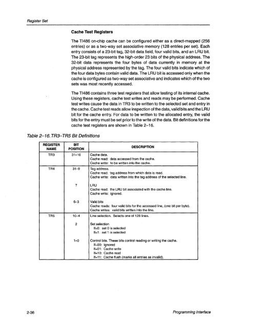
- Page 66 and 67: Register Set 2.3.2.6 Test Registers
- Page 70 and 71: Address Spaces 2.4 Address Spaces T
- Page 72 and 73: Address Spaces 2.4.2 Memory Address
- Page 74 and 75: Address Spaces Figure 2-21. Real Mo
- Page 76 and 77: Address Spaces Figure 2-24. Paging
- Page 78 and 79: Interrupts and Exceptions 2.5 Inter
- Page 80 and 81: Interrupts and Exceptions 2.5.3 Int
- Page 82 and 83: Interrupts and Exceptions Table 2-2
- Page 84 and 85: System Management Mode 2.6 System M
- Page 86 and 87: System Management Mode Figure 2-29.
- Page 88 and 89: System Management Mode The new SMM
- Page 90 and 91: System Management Mode During SMM o
- Page 92 and 93: Protection The Current Privilege Le
- Page 94 and 95: Virtual 8086 Mode 2.9 Virtual 8086
- Page 96 and 97: TI486SLC/E Bus Interface 3-1
- Page 98 and 99: Chapter 3 TI486SLC/E Bus Interface
- Page 100 and 101: Overview Table 3-1. TI486SLCIE Sign
- Page 102 and 103: Overview Table 3-2. Terminal Functi
- Page 104 and 105: Overview Table 3-2. Terminal Functi
- Page 106 and 107: Overview Table 3-2. Terminal Functi
- Page 108 and 109: Overview 3.1.1 Bus Cycle Definition
- Page 110 and 111: Overview Table 3-5 shows the state
- Page 112 and 113: Functional Timing Figure 3-3. Bus A
- Page 114 and 115: Functional Timing 3.2.2.1 Bus Cycle
- Page 116 and 117: Functional Timing Non-Pipelined Wai
- Page 118 and 119:
Functional Timing Because of the de
- Page 120 and 121:
Functional Timing Pipelined Wait St
- Page 122 and 123:
Functional Timing Initiating and Ma
- Page 124 and 125:
Functional Timing Figure 3-12. Comp
- Page 126 and 127:
Functional Timing Figure 3-13. Inte
- Page 128 and 129:
Functional Timing Shutdown Indicati
- Page 130 and 131:
Functional Timing Figure 3-17. Pipe
- Page 132 and 133:
Functional Timing As shown in Figur
- Page 134 and 135:
Functional Timing Figure 3-19. Requ
- Page 136 and 137:
Functional Timing Figure 3-21. Requ
- Page 138 and 139:
Functional Timing Figure 3-22. 8MI
- Page 140 and 141:
Functional Timing HALT Initiated Su
- Page 142 and 143:
Functional Timing 3.2.12 Float Figu
- Page 144 and 145:
TI486DLC/E Bus Interface 4-1
- Page 146 and 147:
Chapter 4 TI486DLC/E Bus Interface
- Page 148 and 149:
Overview Table 4-1. TI486DLCIE SIgn
- Page 150 and 151:
Overview Table 4-2. Terminal Functi
- Page 152 and 153:
Overview Table 4-2. Terminal Functi
- Page 154 and 155:
Overview Table 4-2. Terminal Functi
- Page 156 and 157:
Overview Table 4-6. Signal States D
- Page 158 and 159:
Overview 4.1.2 Power Management 4.1
- Page 160 and 161:
Functional Timing 4.2 Functional Ti
- Page 162 and 163:
Functional Timing The TI486DLC/E da
- Page 164 and 165:
Functional Timing Non-Pipelined Rea
- Page 166 and 167:
Functional Timing Initiating and Ma
- Page 168 and 169:
Functional Timing Figure 4-8. Faste
- Page 170 and 171:
Functional Timing Figure 4-9. Vario
- Page 172 and 173:
Functional Timing Once a pipelined
- Page 174 and 175:
Functional Timing 4.2.3 Bus Cycles
- Page 176 and 177:
Functional Timing Pipelined Cycles
- Page 178 and 179:
Functional Timing LOCK is activated
- Page 180 and 181:
Functional Timing 4.2.6 Halt and Sh
- Page 182 and 183:
Functional Timing Figure 4-17. Pipe
- Page 184 and 185:
Functional Timing Figure 4-19. Non-
- Page 186 and 187:
Functional Timing The TI486DLC/E sa
- Page 188 and 189:
Functional Timing 4.2.9 Hold Acknow
- Page 190 and 191:
Functional Timing Figure 4-23. Requ
- Page 192 and 193:
Functional Timing 4.2.10 Coprocesso
- Page 194 and 195:
Functional Timing 4.2.12 Power Mana
- Page 196 and 197:
Functional Timing Stopping the Inpu
- Page 198 and 199:
Electrical Specifications 5-1
- Page 200 and 201:
Chapter 5 Electrical Specifications
- Page 202 and 203:
ElectricalConnecnons It is recommen
- Page 204 and 205:
Recommended Operating Conditions 5.
- Page 206 and 207:
DC Electrical Characteristics Table
- Page 208 and 209:
AC Characteristics Figure 5-2. TI48
- Page 210 and 211:
AC Characteristics Table 5-9. AC Ch
- Page 212 and 213:
AC Characteristics Table 5-11. AC C
- Page 214 and 215:
____ AC Characteristics 5.5.3 RESET
- Page 216 and 217:
AC Characteristics Figure 5-10. TI4
- Page 218 and 219:
AC Characteristics Figure 5-12. TI4
- Page 220 and 221:
Mechanical Specifications 6-1
- Page 222 and 223:
Chapter 6 Mechanical Specifications
- Page 224 and 225:
Pin Assignments Table 6-1. TI486SLC
- Page 226 and 227:
Pin Assignments Figure 6-3. TI486DL
- Page 228 and 229:
Package Dimensions 6.2 Package Dime
- Page 230 and 231:
Thermal Characteristics 6.3 Thermal
- Page 232 and 233:
Instruction Set 7-1
- Page 234 and 235:
Chapter 7 Instruction Set This sect
- Page 236 and 237:
Instruction Fields 7.2 Instruction
- Page 238 and 239:
Instruction Fields 7.2.5 reg Field
- Page 240 and 241:
Instruction Fields Table 7-7. mod r
- Page 242 and 243:
Instruction Fields 7.2.11 sreg3 Fie
- Page 244 and 245:
Clock Count Summary 7.4 Clock Count
- Page 246 and 247:
--- --;.J -L 01 Table 7-17. Instruc
- Page 248 and 249:
I . ~ -.....J Table 7-17. Instructi
- Page 250 and 251:
Table 7-17. Instructions, Opcodes,
- Page 252 and 253:
Table 7-17. Instructions, Opcodes,
- Page 254 and 255:
-....J N (J.) Table 7-17. Instructi
- Page 256 and 257:
I I i I i Table 7-17. Instructions,
- Page 258 and 259:
...... ...... '" Table 7-17. Instru
- Page 260 and 261:
-....J N co Table 7-17. Instruction
- Page 262 and 263:
"-.I ~ Table 7-17. Instructions, Op
- Page 264 and 265:
Table 7-17. Instructions, Opcodes,
- Page 266 and 267:
U Appendix A TI486 SMM Pro rammer's
- Page 268 and 269:
SMM Implementation A.2 SMM Implemen
- Page 270 and 271:
Figure A-1. SMM Memory Space Header
- Page 272 and 273:
SMM Implementation 6) NMI is the on
- Page 274 and 275:
Instruction Summary A.4 Instruction
- Page 276 and 277:
Instruction Summary A.4.3 Resume No
- Page 278 and 279:
Instruction Summary A.4.6 Save LDTR
- Page 280 and 281:
8MI Handler Example A.5 SMI Handler
- Page 282 and 283:
8MI Handler Example execute_halt: C
- Page 284 and 285:
8MI Handler Example COMMENT A The T
- Page 286 and 287:
8MI Handler Example arrl arr2 arr3
- Page 288 and 289:
.MODEL SMALL . STACK .386P INCLUDE
- Page 290 and 291:
Testing/Debugging SMM Code sgdt COM
- Page 292 and 293:
Testing/Debugging SMM Code i*******
- Page 294 and 295:
TI486 Power Management Features A.7
- Page 296 and 297:
Detection of Tl486 CPU A.9 Detectio
- Page 298 and 299:
Detection of SMM Capable Version A.
- Page 300 and 301:
i**********************************
- Page 302 and 303:
A.11 SMM Feature Comparison SMM Fea
- Page 304 and 305:
SMM Instruction Macros COMMENT A Co
- Page 306 and 307:
SMM Instruction Macros SMM Instruct
- Page 308 and 309:
A.14 Format of Data Used by SVDC/RS
- Page 310 and 311:
Altering SMM Code Limits A.1S Alter
- Page 312 and 313:
SMM Errata A.16 SMM Errata The foll
- Page 314 and 315:
Appendix B TI486 Cache Flush B.1 Ge
- Page 316 and 317:
Appendix C TI486 BIOS Modification
- Page 318 and 319:
Introduction Some example assembler
- Page 320 and 321:
Appendix D Ordering Information 0.1
- Page 322:
~TEXAS INSTRUMENTS Printed in U.S.A