- Page 1 and 2:
SERIES9600 SERVICE MANUAL © April
- Page 3 and 4:
START-UP AND SOFTWARE BOOT Boot Seq
- Page 5 and 6:
SRAM Card Error Codes If an error o
- Page 7 and 8:
Event Codes & Messages The software
- Page 9 and 10:
Event Codes & Messages (Cont.) CODE
- Page 11 and 12:
Event Codes & Messages (Cont.) CODE
- Page 13 and 14:
Event Codes & Messages (Cont.) 57 W
- Page 15 and 16:
Low Battery Charge Messages Under m
- Page 17 and 18:
Error Messages During Operation (Co
- Page 19 and 20:
Status Menu Chart Use the following
- Page 21 and 22:
PIO Status Use this menu to read th
- Page 23 and 24:
Speaker Pitch This menu allows the
- Page 25 and 26:
386 AMI BIOS Post Code Table These
- Page 27 and 28:
386 AMI BIOS Post Code Table (Cont.
- Page 29 and 30:
386 AMI BIOS Post Code Table (Cont.
- Page 31 and 32:
Nobrk.com Error Codes (Executed by
- Page 33 and 34:
Loadip.Exe (Executed By Autoexec.Ba
- Page 35 and 36:
Critical Errors Fatal Errors Code D
- Page 37 and 38:
ii 9600 System Service Manual © De
- Page 39 and 40:
PURPOSE INTRODUCTION This manual co
- Page 41 and 42:
Introduction 3 SAFETY PRECAUTIONS T
- Page 43 and 44:
Introduction 5 EXPLOSION HAZARDS WA
- Page 45 and 46:
Introduction 7 Dangerous Voltage Pr
- Page 47 and 48:
Introduction 9 UNAUTHORIZED MODIFIC
- Page 49 and 50:
OVERVIEW SYSTEM OVERVIEW This secti
- Page 51 and 52:
System Overview 3 • Digital image
- Page 53 and 54:
System Overview 5 • Auto and manu
- Page 55 and 56:
System Overview 7 Video Monitors
- Page 57 and 58:
System Overview 9 System Configurat
- Page 59 and 60:
System Overview 11 NEUROVASCULAR MO
- Page 61 and 62:
System Overview 13 SYSTEM OPERATION
- Page 63 and 64:
System Overview 15 CAMERA ROTATION
- Page 65 and 66:
System Overview 17 WORKSTATION CONT
- Page 67 and 68:
System Overview 19 A V E R A G I N
- Page 69 and 70:
System Overview 21 tab Ctrl Alt HEL
- Page 71 and 72:
System Overview 23 Trackpad Panels
- Page 73 and 74:
System Overview 25 Lenzar Hardcopy
- Page 75 and 76:
System Overview 27 CONTROL PANEL WA
- Page 77 and 78:
System Overview 29 WORKSTATION COVE
- Page 79 and 80:
System Overview 31 3. Pull the left
- Page 81 and 82:
System Overview 33 8. Remove the mo
- Page 83 and 84:
System Overview 35 2. Grasp the top
- Page 85 and 86:
System Overview 37 COMPONENT LOCATI
- Page 87 and 88:
System Overview 39 Mobile C-Arm Com
- Page 89 and 90:
System Overview 41 WORKSTATION COMP
- Page 91 and 92:
System Overview 43 Power/Motor Rela
- Page 93 and 94:
System Overview 45 IR Receiver PCB
- Page 95 and 96:
OVERVIEW POWER DISTRIBUTION The inf
- Page 97 and 98:
Power Distribution 3 WORKSTATION CI
- Page 99 and 100:
Power Distribution 5 WORKSTATION IS
- Page 101 and 102:
Power Distribution 7 POWER CONTROL
- Page 103 and 104:
Power Distribution 9 CB1 CB2 CB3 Fi
- Page 105 and 106:
Power Distribution 11 PS4 (+24 VDC)
- Page 107 and 108:
Power Distribution 13 Figure 8 DC P
- Page 109 and 110:
Power Distribution 15 PS1 (5V and 1
- Page 111 and 112:
Power Distribution 17 115VAC_PH_SW
- Page 113 and 114:
Power Distribution 19 120 VAC DC 7
- Page 115 and 116:
Power Distribution 21 S/N 69-1001 a
- Page 117 and 118:
Power Distribution 23 L N 1 L D 1 G
- Page 119 and 120:
Power Distribution 25 PS2 (24V) S/N
- Page 121 and 122:
Power Distribution 27 Current Sensi
- Page 123 and 124:
Power Distribution 29 Battery Charg
- Page 125 and 126:
Power Distribution 31 S/N 69-1001 a
- Page 127 and 128:
Power Distribution 33 Battery Charg
- Page 129 and 130:
Power Distribution 35 BATTERY RETAI
- Page 131 and 132:
2 C-Arm Control • Mainframe Mothe
- Page 133 and 134:
4 C-Arm Control C-ARM CONTROL PANEL
- Page 135 and 136:
6 C-Arm Control CONTROL PANEL PROCE
- Page 137 and 138:
8 C-Arm Control X-RAY SWITCH The si
- Page 139 and 140:
10 C-Arm Control This illustration
- Page 141 and 142:
12 C-Arm Control 3 C 5 U E5 U1 TP1
- Page 143 and 144:
14 C-Arm Control CARD RACK ASSEMBLI
- Page 145 and 146:
16 C-Arm Control TECHNIQUE PROCESSO
- Page 147 and 148:
18 C-Arm Control 7-Segment Displays
- Page 149 and 150:
20 C-Arm Control ANALOG INTERFACE P
- Page 151 and 152:
22 C-Arm Control X U 4 8 X U 2 0 X
- Page 153 and 154:
24 C-Arm Control A/D SECTION The A/
- Page 155 and 156:
26 C-Arm Control COUNTER/TIMER (CTC
- Page 157 and 158:
28 C-Arm Control BIT # PIN # SIGNAL
- Page 159 and 160:
30 C-Arm Control INTERLOCK SECTION
- Page 161 and 162:
32 C-Arm Control C-ARM MOTHERBOARD
- Page 163 and 164:
34 C-Arm Control 3 E 1 R V 1 L F 8
- Page 165 and 166:
36 C-Arm Control Technique Processo
- Page 167 and 168:
38 C-Arm Control COMMUNICATION BETW
- Page 169 and 170:
2 C-Arm Software LOADING APPLICATIO
- Page 171 and 172:
4 C-Arm Software BOOT SEQUENCE Duri
- Page 173 and 174:
6 C-Arm Software X-RAY CONTROL PANE
- Page 175 and 176:
8 C-Arm Software A - Run Applicatio
- Page 177 and 178:
10 C-Arm Software C - Run Calibrati
- Page 179 and 180:
12 C-Arm Software H - Collimator Ca
- Page 181 and 182:
14 C-Arm Software SRAM FILES The fo
- Page 183 and 184:
16 C-Arm Software SRAM CARD COPY FI
- Page 185 and 186:
18 C-Arm Software HOT-BYTE INFORMAT
- Page 187 and 188:
20 C-Arm Software SRAM BATTERY REPL
- Page 189 and 190:
2 Interlocks / Stator Power Signal
- Page 191 and 192:
4 Interlocks / Stator FAST STOP The
- Page 193 and 194:
6 Interlocks / Stator JUMPER E5/REL
- Page 195 and 196:
8 Interlocks / Stator NORMAL PRE-CH
- Page 197 and 198:
10 Interlocks / Stator STATOR START
- Page 199 and 200:
12 Interlocks / Stator BATTERY CHAR
- Page 201 and 202:
14 Interlocks / Stator POWER SUPPLY
- Page 203 and 204:
OVERVIEW This section describes the
- Page 205 and 206:
X-ray On / Disable 3 X-RAY ENABLE S
- Page 207 and 208:
X-ray On / Disable 5 X-RAY DISABLE
- Page 209 and 210:
OVERVIEW KV GENERATION kV is regula
- Page 211 and 212:
kV Generation 3 The return path for
- Page 213 and 214:
kV Generation 5 KV ERROR CORRECTION
- Page 215 and 216:
kV Generation 7 Figure 3 kV Servo C
- Page 217 and 218:
kV Generation 9 KV GENERATOR FAULTS
- Page 219 and 220:
kV Generation 11 NOTE If the second
- Page 221 and 222:
kV Generation 13 KV ERROR CORRECTIO
- Page 223 and 224:
2 mA Generation CONTROL INPUTS The
- Page 225 and 226:
4 mA Generation FILAMENT REGULATOR
- Page 227 and 228:
6 mA Generation MA SENSE Detects th
- Page 229 and 230:
8 mA Generation MA ERROR LOOP EXAMP
- Page 231 and 232:
10 mA Generation Figure 2 - mA Serv
- Page 233 and 234:
12 mA Generation LOW FLUORO MA The
- Page 235 and 236:
14 mA Generation MA ERROR CORRECTIO
- Page 237 and 238:
2 Generator Calibration During the
- Page 239 and 240:
4 Generator Calibration CALIBRATION
- Page 241 and 242:
6 Generator Calibration EQUIPMENT S
- Page 243 and 244:
8 Generator Calibration 11. Observi
- Page 245 and 246:
10 Generator Calibration mA ZERO R
- Page 247 and 248:
12 Generator Calibration ACCESS CAL
- Page 249 and 250:
14 Generator Calibration DUTY CYCLE
- Page 251 and 252:
16 Generator Calibration KV/MA TECH
- Page 253 and 254:
18 Generator Calibration MERGE EXIS
- Page 255 and 256:
20 Generator Calibration 5R THEORY
- Page 257 and 258:
22 Generator Calibration Example 3
- Page 259 and 260:
24 Generator Calibration 5R ABS TAB
- Page 261 and 262:
26 Generator Calibration 3. Increas
- Page 263 and 264:
28 Generator Calibration NOTE: You
- Page 265 and 266:
30 Generator Calibration B. mA limi
- Page 267 and 268:
32 Generator Calibration 19. Withou
- Page 269 and 270:
34 Generator Calibration 10R ABS TA
- Page 271 and 272:
36 Generator Calibration 10R ENTRAN
- Page 273 and 274:
OVERVIEW MECHANICAL ASSEMBLIES The
- Page 275 and 276:
Mechanical Assemblies 3 HORIZONTAL
- Page 277 and 278:
Mechanical Assemblies 5 MECHANICAL
- Page 279 and 280:
Mechanical Assemblies 7 HORIZONTAL
- Page 281 and 282:
Mechanical Assemblies 9 Figure 5 -
- Page 283 and 284:
Mechanical Assemblies 11 FLIP FLOP
- Page 285 and 286:
Mechanical Assemblies 13 C-ARM BEAR
- Page 287 and 288:
Mechanical Assemblies 15 WIG WAG BR
- Page 289 and 290:
Mechanical Assemblies 17 Figure 8 -
- Page 291 and 292: Mechanical Assemblies 19 REAR CASTE
- Page 293 and 294: Mechanical Assemblies 21 FRONT WHEE
- Page 295 and 296: Mechanical Assemblies 23 REAR WHEEL
- Page 297 and 298: Mechanical Assemblies 25 Older Mode
- Page 299 and 300: Mechanical Assemblies 27 Older Mode
- Page 301 and 302: Mechanical Assemblies 29 Shim Adjus
- Page 303 and 304: Mechanical Assemblies 31 L-ARM ROTA
- Page 305 and 306: Mechanical Assemblies 33 CROSS ARM
- Page 307 and 308: Mechanical Assemblies 35 Figure 16
- Page 309 and 310: Mechanical Assemblies 37 VERTICAL C
- Page 311 and 312: Mechanical Assemblies 39 3. Remove
- Page 313 and 314: 2 Image System Mainframe Motherboar
- Page 315 and 316: 4 Image System IMAGE FUNCTION PCB S
- Page 317 and 318: 6 Image System ������
- Page 319 and 320: 8 Image System COLLIMATOR OVERVIEW
- Page 321 and 322: 10 Image System IRIS MOTOR The coll
- Page 323 and 324: 12 Image System LEAF IN/OUT MOTOR T
- Page 325 and 326: 14 Image System LEAF ROTATION MOTOR
- Page 327 and 328: 16 Image System COLLIMATOR ERROR ME
- Page 329 and 330: 18 Image System IMAGE INTENSIFIER O
- Page 331 and 332: 20 Image System WARNING... Image in
- Page 333 and 334: 22 Image System CCD CAMERA OVERVIEW
- Page 335 and 336: 24 Image System Invert Image/ Rever
- Page 337 and 338: 26 Image System ������
- Page 339 and 340: 28 Image System ������
- Page 341: 30 Image System Anti-Vignetting A s
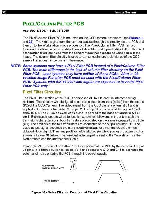
- Page 345 and 346: 34 Image System PIXEL FILTER PCB As
- Page 347 and 348: 36 Image System CCD CAMERA REPLACEM
- Page 349 and 350: 38 Image System CCD CAMERA REPLACEM
- Page 351 and 352: 40 Image System VIDEO LEVEL INDICAT
- Page 353 and 354: 42 Image System ��� ���
- Page 355 and 356: 44 Image System STATOR THERMAL CUTO
- Page 357 and 358: 46 Image System REPLACEMENT OF HIGH
- Page 359 and 360: IMAGE SYSTEM CALIBRATION The proced
- Page 361 and 362: Image System Calibration 3 TOOLS Th
- Page 363 and 364: Image System Calibration 5 4. Attac
- Page 365 and 366: Image System Calibration 7 CALIBRAT
- Page 367 and 368: Image System Calibration 9 10. With
- Page 369 and 370: Image System Calibration 11 CONFIRM
- Page 371 and 372: Image System Calibration 13 ADJUST
- Page 373 and 374: Image System Calibration 15 8. Sele
- Page 375 and 376: Image System Calibration 17 Figure
- Page 377 and 378: Image System Calibration 19 4. If t
- Page 379 and 380: Image System Calibration 21 270° 0
- Page 381 and 382: Image System Calibration 23 ADJUST
- Page 383 and 384: Image System Calibration 25 COLLIMA
- Page 385 and 386: Image System Calibration 27 NOTE: I
- Page 387 and 388: Image System Calibration 29 VARIABL
- Page 389 and 390: Image System Calibration 31 9. Sele
- Page 391 and 392: Image System Calibration 33 BEAM AL
- Page 393 and 394:
Image System Calibration 35 C. Swin
- Page 395 and 396:
Image System Calibration 37 Adjust
- Page 397 and 398:
Image System Calibration 39 PIXEL/C
- Page 399 and 400:
Image System Calibration 41 ANTI-VI
- Page 401 and 402:
OVERVIEW WORKSTATION CONTROL This s
- Page 403 and 404:
Workstation Control 3 CONTROL PANEL
- Page 405 and 406:
Workstation Control 5 CONTROL PANEL
- Page 407 and 408:
Workstation Control 7 Figure 3 - Wo
- Page 409 and 410:
Workstation Control 9 ELECTRONICS B
- Page 411 and 412:
Workstation Control 11 AUXILIARY IN
- Page 413 and 414:
Workstation Control 13 X-RAY DISABL
- Page 415 and 416:
Workstation Control 15 COMMUNICATIO
- Page 417 and 418:
Workstation Control 17 OPTION PROM
- Page 419 and 420:
Workstation Control 19 386 AT MOTHE
- Page 421 and 422:
Workstation Control 21 IR (INFRARED
- Page 423 and 424:
Workstation Control 23 If the pulse
- Page 425 and 426:
Workstation Control 25 IR RECEIVER
- Page 427 and 428:
Workstation Control 27 Older Style
- Page 429 and 430:
Workstation Control 29 INTERCONNECT
- Page 431 and 432:
2 Workstation Software WORKSTATION
- Page 433 and 434:
4 Workstation Software FRONT PANEL
- Page 435 and 436:
6 Workstation Software TOGGLE MOTIO
- Page 437 and 438:
8 Workstation Software Qwerty Keys
- Page 439 and 440:
10 Workstation Software Track Pad K
- Page 441 and 442:
12 Workstation Software Front Panel
- Page 443 and 444:
14 Workstation Software Tone Contro
- Page 445 and 446:
16 Workstation Software Watchdog Re
- Page 447 and 448:
Video Path 2 REFERENCE SCHEMATICS T
- Page 449 and 450:
Video Path 4 HIGH SCAN NON INTERLAC
- Page 451 and 452:
Video Path 6 WORKSTATION The video
- Page 453 and 454:
Video Path 8 Auxiliary Interface PC
- Page 455 and 456:
Video Path 10 Peripherals Analog in
- Page 457 and 458:
Video Path 12 HARD COPY CAMERA Vide
- Page 459 and 460:
Video Path 14 Auxiliary Interface P
- Page 461 and 462:
Video Path 16 Video Switching PCB O
- Page 463 and 464:
Video Path 18 Scan Converter PCB Fi
- Page 465 and 466:
2 Video Control IMAGE PROCESSOR PCB
- Page 467 and 468:
4 Video Control IMAGE PROCESSOR TES
- Page 469 and 470:
6 Video Control VIDEO SWITCHING PCB
- Page 471 and 472:
8 Video Control 50/60 HZ VIDEO CONT
- Page 473 and 474:
10 Video Control FAST SCAN MONITORS
- Page 475 and 476:
12 Video Control CONTRAST AND BRIGH
- Page 477 and 478:
14 Video Control HIGH SCAN BRIGHTNE
- Page 479 and 480:
2 Image Storage IDE HARD DISK DRIVE
- Page 481 and 482:
4 Image Storage 30FPS SCSI DISK OPT
- Page 483 and 484:
6 Image Storage 4/30 FPS SCSI DISK
- Page 485 and 486:
8 Image Storage 14. The following w
- Page 487 and 488:
Image Storage DEBUGGING USING IP-SC
- Page 489 and 490:
12 Image Storage �� �� �
- Page 491 and 492:
14 Image Storage Figure 7 - SCSI Di
- Page 493 and 494:
16 Image Storage Figure 9 - IP-SCSI
- Page 495 and 496:
18 Image Storage � � � �
- Page 497 and 498:
20 Image Storage ������
- Page 499 and 500:
2 Peripherals Figure 1 - Rear Panel
- Page 501 and 502:
4 Peripherals RECORD UNPROCESSED VI
- Page 503 and 504:
6 Peripherals VCR CONNECTIONS To en
- Page 505 and 506:
8 Peripherals HARD COPY CAMERA Imag
- Page 507 and 508:
10 Peripherals MOUNTING INFORMATION
- Page 509 and 510:
12 Peripherals DIGITAL LASER CAMERA
- Page 511 and 512:
14 Peripherals 6. When CUSTOMIZE OP
- Page 513 and 514:
16 Peripherals Digital Laser Camera
- Page 515 and 516:
18 Peripherals After the unit has b
- Page 517 and 518:
20 Peripherals 3. Then, select a sp
- Page 519 and 520:
22 Peripherals 4. Move the cursor t
- Page 521 and 522:
2 Appendix PAINT KITS PART NUMBER D
- Page 523 and 524:
4 Appendix SPECIFICATIONS & TOLERAN
- Page 525 and 526:
UPDATE 12-INCH IMAGE SYSTEM 9600 SY
- Page 527 and 528:
00 Imaging Workstation Service Manu
- Page 529 and 530:
9600 Imaging Workstation Service Ma
- Page 531 and 532:
9600 Imaging Workstation Service Ma
- Page 533 and 534:
9600 Imaging Workstation Service Ma
- Page 535 and 536:
9600 Imaging Workstation Service Ma
- Page 537 and 538:
9600 Imaging Workstation Service Ma
- Page 539 and 540:
9600 Imaging Workstation Service Ma
- Page 541 and 542:
9600 Imaging Workstation Service Ma
- Page 543 and 544:
9600 Imaging Workstation Service Ma
- Page 545 and 546:
9600 Imaging Workstation Service Ma