

Molecular beam epitaxial growth of III-V semiconductor ... - KOBRA
Molecular beam epitaxial growth of III-V semiconductor ... - KOBRA
Molecular beam epitaxial growth of III-V semiconductor ... - KOBRA

You also want an ePaper? Increase the reach of your titles
YUMPU automatically turns print PDFs into web optimized ePapers that Google loves.
MBE Growth <strong>of</strong> Self-Assembled InAs and InGaAs Quantum Dots Embedded in<br />
Silicon Matrix<br />
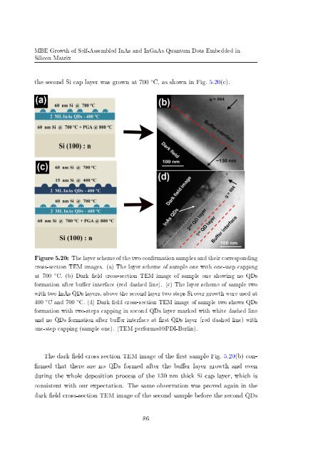
the second Si cap layer was grown at 700 ◦ C, as shown in Fig. 5.20(c).<br />
Figure 5.20: The layer scheme <strong>of</strong> the two conrmation samples and their corresponding<br />
cross-section TEM images. (a) The layer scheme <strong>of</strong> sample one with one-step capping<br />
at 700 ◦ C. (b) Dark eld cross-section TEM image <strong>of</strong> sample one showing no QDs<br />
formation after buer interface (red dashed line). (c) The layer scheme <strong>of</strong> sample two<br />
with two InAs QDs layers, above the second layer two steps Si over <strong>growth</strong> were used at<br />
400 ◦ C and 700 ◦ C. (d) Dark eld cross-section TEM image <strong>of</strong> sample two shows QDs<br />
formation with two-steps capping in second QDs layer marked with white dashed line<br />
and no QDs formation after buer interface at rst QDs layer (red dashed line) with<br />
one-step capping (sample one). (TEM performed@PDI-Berlin).<br />
The dark eld cross section TEM image <strong>of</strong> the rst sample Fig. 5.20(b) con-<br />
rmed that there are no QDs formed after the buer layer <strong>growth</strong> and even<br />
during the whole deposition process <strong>of</strong> the 130 nm thick Si cap layer, which is<br />
consistent with our expectation. The same observation was proved again in the<br />
dark eld cross-section TEM image <strong>of</strong> the second sample before the second QDs<br />
86


