

Molecular beam epitaxial growth of III-V semiconductor ... - KOBRA
Molecular beam epitaxial growth of III-V semiconductor ... - KOBRA
Molecular beam epitaxial growth of III-V semiconductor ... - KOBRA

Create successful ePaper yourself
Turn your PDF publications into a flip-book with our unique Google optimized e-Paper software.
Experimental Growth and Characterization Techniques<br />
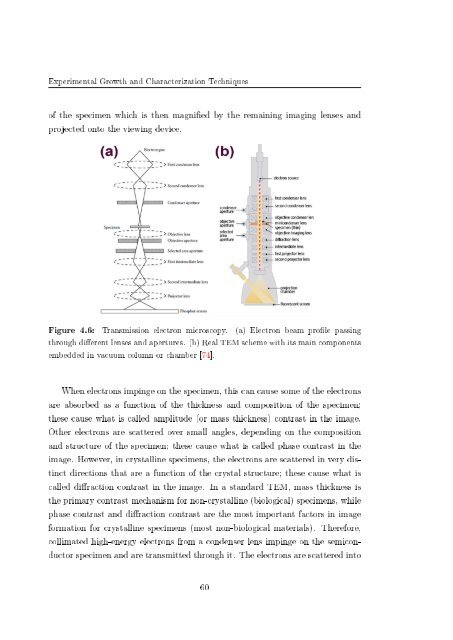
<strong>of</strong> the specimen which is then magnied by the remaining imaging lenses and<br />
projected onto the viewing device.<br />
Figure 4.6: Transmission electron microscopy. (a) Electron <strong>beam</strong> prole passing<br />
through dierent lenses and apertures. (b) Real TEM scheme with its main components<br />
embedded in vacuum column or chamber [74].<br />
When electrons impinge on the specimen, this can cause some <strong>of</strong> the electrons<br />
are absorbed as a function <strong>of</strong> the thickness and composition <strong>of</strong> the specimen;<br />
these cause what is called amplitude (or mass thickness) contrast in the image.<br />
Other electrons are scattered over small angles, depending on the composition<br />
and structure <strong>of</strong> the specimen; these cause what is called phase contrast in the<br />
image. However, in crystalline specimens, the electrons are scattered in very distinct<br />
directions that are a function <strong>of</strong> the crystal structure; these cause what is<br />
called diraction contrast in the image. In a standard TEM, mass thickness is<br />
the primary contrast mechanism for non-crystalline (biological) specimens, while<br />
phase contrast and diraction contrast are the most important factors in image<br />
formation for crystalline specimens (most non-biological materials). Therefore,<br />
collimated high-energy electrons from a condenser lens impinge on the <strong>semiconductor</strong><br />
specimen and are transmitted through it. The electrons are scattered into<br />
60


