

Molecular beam epitaxial growth of III-V semiconductor ... - KOBRA
Molecular beam epitaxial growth of III-V semiconductor ... - KOBRA
Molecular beam epitaxial growth of III-V semiconductor ... - KOBRA

You also want an ePaper? Increase the reach of your titles
YUMPU automatically turns print PDFs into web optimized ePapers that Google loves.
Optimization <strong>of</strong> MEE and MBE <strong>growth</strong> <strong>of</strong> GaP Buer on Silicon Substrate<br />
were varied while maintaining a 100 nm/h <strong>growth</strong> rate, as was done during the<br />
GaP/GaP homoepitaxy <strong>growth</strong> optimization [136]. The GaP-MBE/GaP-MEE/<br />
Si was grown on cleaned silicon substrate as described in Sec. 7.3 in conjunction<br />
with GaP-MEE <strong>growth</strong> procedure discussed in Sec. 7.4.1. AFM and RHEED<br />
analysis were used to verify the 2D planar <strong>growth</strong> and investigate the surface<br />
morphology <strong>of</strong> the dierent GaP <strong>growth</strong> modes.<br />
7.5.1 Growth Temperature <strong>of</strong> MBE-GaP<br />
After the <strong>growth</strong> <strong>of</strong> the rst 10 nm GaP using the MEE-mode, the <strong>growth</strong> temperature<br />
<strong>of</strong> the MBE step was varied with a narrow range <strong>of</strong> 20 K from the<br />
standard <strong>growth</strong> temperature <strong>of</strong> GaP on GaP substrate in the MBE-GaP <strong>growth</strong><br />
[136]. The Ga <strong>growth</strong> rate used for the MBE was the same as for the MEE step<br />
(100 nm/h) and P 2 /Ga ratio was set to 15. Two samples were overgrown with<br />
40 nm GaP (nominal thickness) at two dierent <strong>growth</strong> temperatures <strong>of</strong> 545 ◦ C<br />
and 560 ◦ C, respectively. The surface reconstruction during MEE and MBE GaP<br />
epitaxy was in-situ monitored with by RHEED. Note that between MEE-GaP<br />
<strong>growth</strong> step and MBE-GaP <strong>growth</strong> there is a <strong>growth</strong> stop, where the substrate<br />
temperature was ramped up from 350 ◦ C (MEE-step) to the MBE-GaP <strong>growth</strong><br />
temperature with a ramp rate <strong>of</strong> 50 K/min.<br />
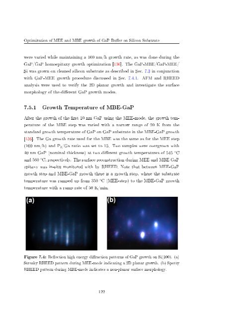
Figure 7.4: Reection high energy diraction patterns <strong>of</strong> GaP <strong>growth</strong> on Si(100). (a)<br />
Streaky RHEED pattern during MEE-mode indicating a 2D planar <strong>growth</strong>. (b) Spotty<br />
RHEED pattern during MBE-mode indicates a non-planar surface morphology.<br />
122


