

Molecular beam epitaxial growth of III-V semiconductor ... - KOBRA
Molecular beam epitaxial growth of III-V semiconductor ... - KOBRA
Molecular beam epitaxial growth of III-V semiconductor ... - KOBRA

Create successful ePaper yourself
Turn your PDF publications into a flip-book with our unique Google optimized e-Paper software.
Introduction<br />
1.1.2 Thesis Approach<br />
The successful integration <strong>of</strong> the <strong>III</strong>-V materials on silicon holds a great promise<br />
for the future demonstration <strong>of</strong> the practical integrated <strong>III</strong>-V optoelectronic devices<br />
on a Si CMOS platform. In particular, optical interconnect systems provide<br />
a promising approach for the realization <strong>of</strong> the next generation high-speed communication<br />
and computing technologies [11]. However, compatibility with microelectronic<br />
fabrication technologies is very limited. Our approach is to combine<br />
the superior passive optical properties <strong>of</strong> silicon with the superior optical emission<br />
properties <strong>of</strong> <strong>III</strong>-V material by reducing the amount <strong>of</strong> <strong>III</strong>-V materials to the very<br />
limit <strong>of</strong> the active region or by embedding the active layer (<strong>III</strong>-V quantum dots or<br />
dashes nanostructures) in <strong>III</strong>-V matrix using the minimum amount <strong>of</strong> <strong>III</strong>-V materials<br />
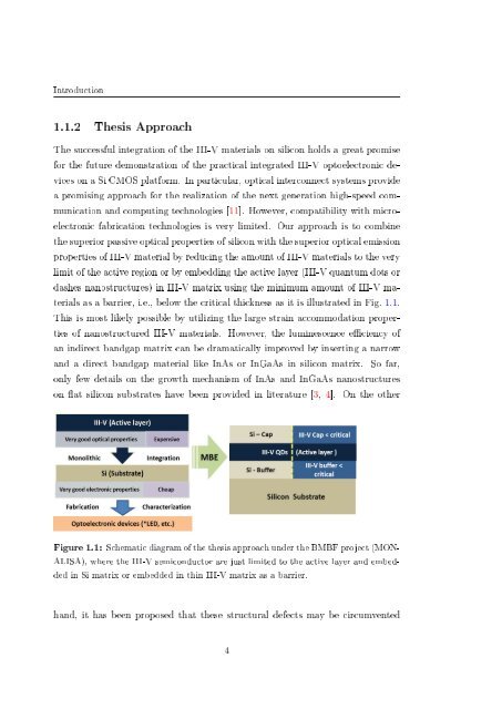
as a barrier, i.e., below the critical thickness as it is illustrated in Fig. 1.1.<br />
This is most likely possible by utilizing the large strain accommodation properties<br />
<strong>of</strong> nanostructured <strong>III</strong>-V materials. However, the luminescence eciency <strong>of</strong><br />
an indirect bandgap matrix can be dramatically improved by inserting a narrow<br />
and a direct bandgap material like InAs or InGaAs in silicon matrix. So far,<br />
only few details on the <strong>growth</strong> mechanism <strong>of</strong> InAs and InGaAs nanostructures<br />
on at silicon substrates have been provided in literature [3, 4]. On the other<br />
Figure 1.1: Schematic diagram <strong>of</strong> the thesis approach under the BMBF project (MON-<br />
ALISA), where the <strong>III</strong>-V <strong>semiconductor</strong> are just limited to the active layer and embedded<br />
in Si matrix or embedded in thin <strong>III</strong>-V matrix as a barrier.<br />
hand, it has been proposed that these structural defects may be circumvented<br />
4


