

Molecular beam epitaxial growth of III-V semiconductor ... - KOBRA
Molecular beam epitaxial growth of III-V semiconductor ... - KOBRA
Molecular beam epitaxial growth of III-V semiconductor ... - KOBRA

Create successful ePaper yourself
Turn your PDF publications into a flip-book with our unique Google optimized e-Paper software.
MBE Growth <strong>of</strong> Self-Assembled InAs and InGaAs Quantum Dots Embedded in<br />
Silicon Matrix<br />
carried out at constant voltage <strong>of</strong> 1 V , while the current was measured at different<br />
stripe distances. The I-V curve was recorded and the doping level was<br />
calculated for dierent As 4 uxes. Fig. 5.32 shows the doping level dependence<br />
with the BEP As 4 ux. A linear carrier concentration dependence on As 4 ux<br />
was observed up to a doping level <strong>of</strong> 7.28 × 10 17 cm −3 for a As 4 <strong>of</strong> BEP value<br />
3.6 × 10 −8 Torr. A new series <strong>of</strong> samples were studied by keeping the As ux<br />
constant at 1.2 × 10 −8 Torr but with increasing the layer thickness from 100 nm<br />
to 200 nm.<br />
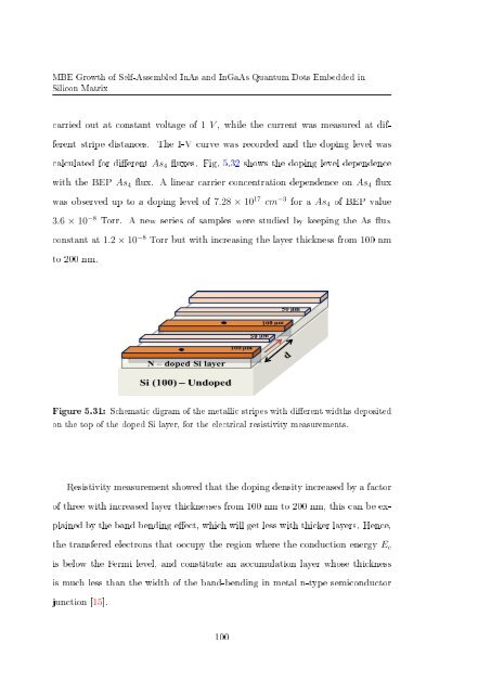
Figure 5.31: Schematic digram <strong>of</strong> the metallic stripes with dierent widths deposited<br />
on the top <strong>of</strong> the doped Si layer, for the electrical resistivity measurements.<br />
Resistivity measurement showed that the doping density increased by a factor<br />
<strong>of</strong> three with increased layer thicknesses from 100 nm to 200 nm, this can be explained<br />
by the band bending eect, which will get less with thicker layers. Hence,<br />
the transfered electrons that occupy the region where the conduction energy E c<br />
is below the Fermi level, and constitute an accumulation layer whose thickness<br />
is much less than the width <strong>of</strong> the band-bending in metal n-type <strong>semiconductor</strong><br />
junction [15].<br />
100


