

Molecular beam epitaxial growth of III-V semiconductor ... - KOBRA
Molecular beam epitaxial growth of III-V semiconductor ... - KOBRA
Molecular beam epitaxial growth of III-V semiconductor ... - KOBRA

You also want an ePaper? Increase the reach of your titles
YUMPU automatically turns print PDFs into web optimized ePapers that Google loves.
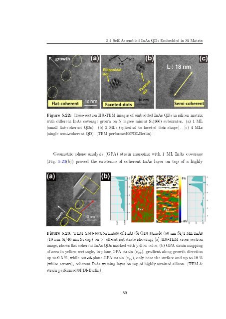
5.4 Self-Assembled InAs QDs Embedded in Si Matrix<br />
Figure 5.22: Cross-section HR-TEM images <strong>of</strong> embedded InAs QDs in silicon matrix<br />
with dierent InAs coverage grown on 5 degree miscut Si(100) substrates. (a) 1 ML<br />
(small at-coherent QDs). (b) 2 MLs (spherical to faceted dots shape). (c) 4 MLs<br />
(single semi-coherent QD). (TEM performed@PDI-Berlin).<br />
Geometric phase analysis (GPA) strain mapping with 1 ML InAs coverage<br />
(Fig. 5.23(b)) proved the existence <strong>of</strong> coherent InAs layer on top <strong>of</strong> a highly<br />
Figure 5.23: TEM cross-section image <strong>of</strong> InAs/Si QDs sample (50 nm Si/1 ML InAs<br />
/10 nm Si/40 nm Si cap) on 5 ◦ o-cut substrate showing; (a) HR-TEM cross section<br />
image, shows at coherent InAs QDs marked with yellow color; (b) GPA strain mapping<br />
<strong>of</strong> area in yellow rectangle, in-plane GPA strain (e xx ), gradient along <strong>growth</strong> direction<br />
up to 0.5 %, while out-<strong>of</strong>-plane GPA strain (e yy ), only near the surface and up to 10 %<br />
(white arrows), coherent InAs wetting layer on top <strong>of</strong> highly strained silicon. (TEM &<br />
strain performed@PDI-Berlin).<br />
89


