

Molecular beam epitaxial growth of III-V semiconductor ... - KOBRA
Molecular beam epitaxial growth of III-V semiconductor ... - KOBRA
Molecular beam epitaxial growth of III-V semiconductor ... - KOBRA

Create successful ePaper yourself
Turn your PDF publications into a flip-book with our unique Google optimized e-Paper software.
6.3 Further Results: Site-Controlled Growth <strong>of</strong> InGaAs QDs Embedded in GaAs<br />
Matrix on Pre-Patterned Silicon Substrate<br />
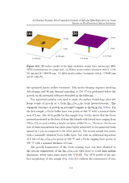
Figure 6.5:<br />
3D surface prole <strong>of</strong> the high resolution atomic force microscopy (HR-<br />
AFM) measurements <strong>of</strong> a single hole. (a) Before in-situ surface treatment with L =(70-<br />
75) nm and D =(60-70) nm. (b) After in-situ surface treatment with L =(70-80) nm<br />
and D =(65-70).<br />
the optimized in-situ surface treatment. This in-situ cleaning sequence involving<br />
AH cleaning and 30 min thermal annealing at 750 ◦ C was performed before the<br />
<strong>growth</strong> on all patterned substrate described in the following.<br />
Two patterned samples were used to study the surface morphology after different<br />
stages <strong>of</strong> <strong>growth</strong> <strong>of</strong> a GaAs/In 0.15 Ga 0.85 As/GaAs heterostructure. The<br />
schematic sequence <strong>of</strong> <strong>growth</strong> on patterned samples is shown in Fig. 6.6(a). For<br />
the rst sample, a GaAs buer layer was grown at 600 ◦ C with a nominal thickness<br />
<strong>of</strong> 2 nm. The AFM prole for this sample (Fig. 6.6(b)) shows that the GaAs<br />
material nucleated in the form <strong>of</strong> dome like islands with lateral sizes ranging from<br />
120 to 175 nm and exhibits a height variation <strong>of</strong> 60-115 nm. Moreover, the formation<br />
<strong>of</strong> these nano-islands has taken place highly selectively in the patterned holes<br />
spaced by 1 µm as compared to the other periods. The second sample was grown<br />
with a nominally identical GaAs buer layer, but with an additional deposition<br />
<strong>of</strong> 2 MLs <strong>of</strong> In 0.15 Ga 0.85 As grown at 500 ◦ C and a GaAs capping layer grown at<br />
500 ◦ C with a nominal thickness <strong>of</strong> 2 nm.<br />
The <strong>growth</strong> temperature <strong>of</strong> the GaAs capping layer was kept identical to<br />
the <strong>growth</strong> temperature <strong>of</strong> the In 0.15 Ga 0.85 As QDs layer to avoid high indium<br />
desorption, which takes place above 500 ◦ C [100]. The AFM prole <strong>of</strong> the surface<br />
morphology <strong>of</strong> this sample (Fig. 6.6(c,d)) conrms the continuation <strong>of</strong> site-<br />
111


