

Molecular beam epitaxial growth of III-V semiconductor ... - KOBRA
Molecular beam epitaxial growth of III-V semiconductor ... - KOBRA
Molecular beam epitaxial growth of III-V semiconductor ... - KOBRA

Create successful ePaper yourself
Turn your PDF publications into a flip-book with our unique Google optimized e-Paper software.
3.4 Challenges <strong>of</strong> Hetero<strong>epitaxial</strong> Growth <strong>of</strong> <strong>III</strong>-V on Silicon<br />
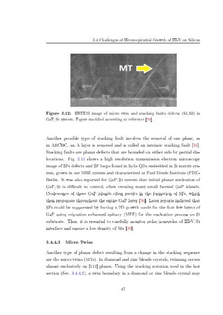
Figure 3.12:<br />
HRTEM image <strong>of</strong> micro twin and stacking faults defects (S1,S2) in<br />
GaP/Si system. Figure modied according to reference [70].<br />
Another possible type <strong>of</strong> stacking fault involves the removal <strong>of</strong> one plane, as<br />
in ABCBC, an A layer is removed and is called an intrinsic stacking fault [31].<br />
Stacking faults are planar defects that are bounded on either side by partial dislocations.<br />
Fig. 3.11 shows a high resolution transmission electron microscopy<br />
image <strong>of</strong> SFs defects and SF loops found in InAs QDs embedded in Si matrix system,<br />
grown in our MBE system and characterized at Paul Drude Institute (PDI)-<br />
Berlin. It was also reported for GaP/Si system that initial planar nucleation <strong>of</strong><br />
GaP/Si is dicult to control, <strong>of</strong>ten creating many small faceted GaP islands.<br />
Coalescence <strong>of</strong> these GaP islands <strong>of</strong>ten results in the formation <strong>of</strong> SFs, which<br />
then propagate throughout the entire GaP layer [70]. Later reports indicted that<br />
SFs could be suppressed by forcing a 2D <strong>growth</strong> mode for the rst few layers <strong>of</strong><br />
GaP using migration enhanced epitaxy (MEE) for the nucleation process on Si<br />
substrate. Thus, it is essential to carefully monitor polar/non-polar <strong>of</strong> <strong>III</strong>-V/Si<br />
interface and ensure a low density <strong>of</strong> SFs [39].<br />
3.4.4.3 Micro Twins<br />
Another type <strong>of</strong> planar defect resulting from a change in the stacking sequence<br />
are the micro twins (MTs). In diamond and zinc blende crystals, twinning occurs<br />
almost exclusively on [111] planes. Using the stacking notation used in the last<br />
section (Sec. 3.4.4.2), a twin boundary in a diamond or zinc blende crystal may<br />
47


