

Molecular beam epitaxial growth of III-V semiconductor ... - KOBRA
Molecular beam epitaxial growth of III-V semiconductor ... - KOBRA
Molecular beam epitaxial growth of III-V semiconductor ... - KOBRA

You also want an ePaper? Increase the reach of your titles
YUMPU automatically turns print PDFs into web optimized ePapers that Google loves.
MBE Growth <strong>of</strong> Self-Assembled InAs and InGaAs Quantum Dots Embedded in<br />
Silicon Matrix<br />
= 6 kV, <strong>growth</strong> temperature = 700 ◦ C for both samples and only the time for<br />
each sample was varied.<br />
Sample No. Sample 1 Sample 2<br />
Growth parameter<br />
Growth rate Thickness Growth rate Thickness<br />
[nm/h] [nm] [nm/h] [nm]<br />
Deposition controller<br />
140 100 135 50<br />
Prolometer 310 220 290 115<br />
Table 5.1:<br />
Calibration <strong>of</strong> electron <strong>beam</strong> evaporator (EBE) silicon cell using two different<br />
samples.<br />
Table 5.6 shows the calibration parameters <strong>of</strong> the grown samples. The average<br />
tooling factor according to Eq. 5.6 was found equal to 225.<br />
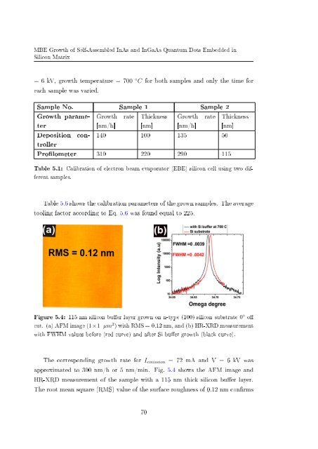
Figure 5.4: 115 nm silicon buer layer grown on n-type (100) silicon substrate 0 ◦ o<br />
cut. (a) AFM image (1×1 µm 2 ) with RMS = 0.12 nm, and (b) HR-XRD measurement<br />
with FWHM values before (red curve) and after Si buer <strong>growth</strong> (black curve).<br />
The corresponding <strong>growth</strong> rate for I emission = 72 mA and V = 6 kV was<br />
approximated to 300 nm/h or 5 nm/min. Fig. 5.4 shows the AFM image and<br />
HR-XRD measurement <strong>of</strong> the sample with a 115 nm thick silicon buer layer.<br />
The root mean square (RMS) value <strong>of</strong> the surface roughness <strong>of</strong> 0.12 nm conrms<br />
70


