

Molecular beam epitaxial growth of III-V semiconductor ... - KOBRA
Molecular beam epitaxial growth of III-V semiconductor ... - KOBRA
Molecular beam epitaxial growth of III-V semiconductor ... - KOBRA

You also want an ePaper? Increase the reach of your titles
YUMPU automatically turns print PDFs into web optimized ePapers that Google loves.
MBE Growth <strong>of</strong> Self-Assembled InAs and InGaAs Quantum Dots Embedded in<br />
Silicon Matrix<br />
followed by dry and wet etching possibly cause serious crystalline damages and<br />
some external chemical impurities [16].<br />
5.4.1 Experimental Details<br />
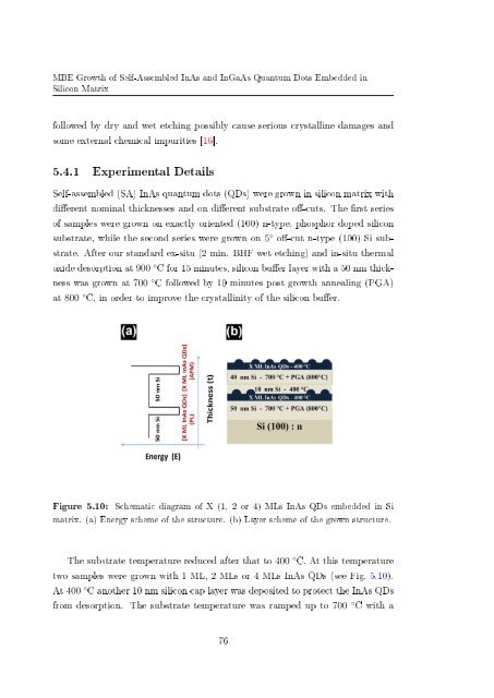
Self-assembled (SA) InAs quantum dots (QDs) were grown in silicon matrix with<br />
dierent nominal thicknesses and on dierent substrate o-cuts. The rst series<br />
<strong>of</strong> samples were grown on exactly oriented (100) n-type, phosphor doped silicon<br />
substrate, while the second series were grown on 5 ◦ o-cut n-type (100) Si substrate.<br />
After our standard ex-situ (2 min. BHF wet etching) and in-situ thermal<br />
oxide desorption at 900 ◦ C for 15 minutes, silicon buer layer with a 50 nm thickness<br />
was grown at 700 ◦ C followed by 10 minutes post <strong>growth</strong> annealing (PGA)<br />
at 800 ◦ C, in order to improve the crystallinity <strong>of</strong> the silicon buer.<br />
Figure 5.10:<br />
Schematic diagram <strong>of</strong> X (1, 2 or 4) MLs InAs QDs embedded in Si<br />
matrix. (a) Energy scheme <strong>of</strong> the structure. (b) Layer scheme <strong>of</strong> the grown structure.<br />
The substrate temperature reduced after that to 400 ◦ C. At this temperature<br />
two samples were grown with 1 ML, 2 MLs or 4 MLs InAs QDs (see Fig. 5.10).<br />
At 400 ◦ C another 10 nm silicon cap layer was deposited to protect the InAs QDs<br />
from desorption. The substrate temperature was ramped up to 700 ◦ C with a<br />
76


