

Molecular beam epitaxial growth of III-V semiconductor ... - KOBRA
Molecular beam epitaxial growth of III-V semiconductor ... - KOBRA
Molecular beam epitaxial growth of III-V semiconductor ... - KOBRA

You also want an ePaper? Increase the reach of your titles
YUMPU automatically turns print PDFs into web optimized ePapers that Google loves.
5.3 Results and Discussion<br />
the smoothness <strong>of</strong> the silicon buer layer, compared with an RMS value <strong>of</strong> 0.24<br />
nm <strong>of</strong> the substrate before Si buer layer <strong>growth</strong>. On the other hand, the HR-<br />
XRD measurements show almost the same full width at half maximum (FWHM)<br />
value indicating together with TEM measurements (shown later) a very good<br />
crystalline quality <strong>of</strong> the Si buer layer. This in turns resulted in additional<br />
improvement in surface quality and creating a fresh Si surface ready for further<br />
<strong>III</strong>-V deposition.<br />
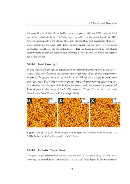
5.3.3.2 InAs Coverage<br />
In this section the amount <strong>of</strong> deposited InAs material was varied in the range <strong>of</strong> 2 -<br />
5 MLs. The rest <strong>of</strong> <strong>growth</strong> parameters are: V/<strong>III</strong> ratio <strong>of</strong> 25, <strong>growth</strong> temperature<br />
= 400 ◦ C, In <strong>growth</strong> rate = 108 nm/h (= 0.1 ML/s) on n-doped Si (100) were<br />
kept the same. Fig 5.5 shows clear size and density dependence on InAs coverage.<br />
The density and the size <strong>of</strong> InAs QDs increased with the increasing amount <strong>of</strong><br />
InAs deposit in the range <strong>of</strong> 2 - 5 MLs from ∼ 10 10 cm −2 to ∼ 10 11 cm −2 and<br />
lateral sizes from 15 nm to 40 nm, respectively.<br />
Figure 5.5: (1 × 1 µm 2 ) AFM images <strong>of</strong> InAs QDs with dierent InAs coverage. (a)<br />
2 MLs InAs, (b) 3 MLs InAs, and (c) 5 ML InAs.<br />
5.3.3.3 Growth Temperature<br />
The <strong>growth</strong> parameters used in this section are: V/<strong>III</strong> ratio <strong>of</strong> 25, 2 MLs InAs<br />
coverage, In <strong>growth</strong> rate = 108 nm/h (= 0.1 ML/s) on n-doped Si (100) substrate<br />
71


