

Molecular beam epitaxial growth of III-V semiconductor ... - KOBRA
Molecular beam epitaxial growth of III-V semiconductor ... - KOBRA
Molecular beam epitaxial growth of III-V semiconductor ... - KOBRA

Create successful ePaper yourself
Turn your PDF publications into a flip-book with our unique Google optimized e-Paper software.
6.2 MBE Growth <strong>of</strong> SA-InAs Quantum Dots Embedded in Thin GaAs Matrix on Flat<br />
Silicon Substrate<br />
to Asai et al. [111], even after the deposition <strong>of</strong> a GaAs layer with an average<br />
thickness <strong>of</strong> 1 ML to 2 MLs <strong>of</strong> GaAs onto Si, reections patterns obtained from<br />
RHEED conrmed the onset <strong>of</strong> the islanding mechanism <strong>growth</strong>. An AFM study<br />
revealed the formation on this surface <strong>of</strong> lens shaped islands at a density <strong>of</strong><br />
about ∼ 10 11 cm −2 . A further increase in the average thickness <strong>of</strong> the GaAs<br />
layer has little eect on the shapes <strong>of</strong> the islands, which can be seen in the cross<br />
sections <strong>of</strong> these structures, as it has been presented from dierent research groups<br />
[112, 113, 114].<br />
6.2.2 MBE Epitaxy <strong>of</strong> InAs/GaAs/Si Structure<br />
A misoriented n-type silicon substrate with 5 ◦ o-cut underwent our standard<br />
ex-situ (BHF wet etching for 2 min.), and in-situ (thermal oxide desorption at<br />
870 ◦ C for 15 min.) surface treatment. The use <strong>of</strong> missoriented substrate has<br />
been successfully proved that it has signicant inuence on anti-phase domains<br />
suppression by means <strong>of</strong> double-layer step formation [115, 67].<br />
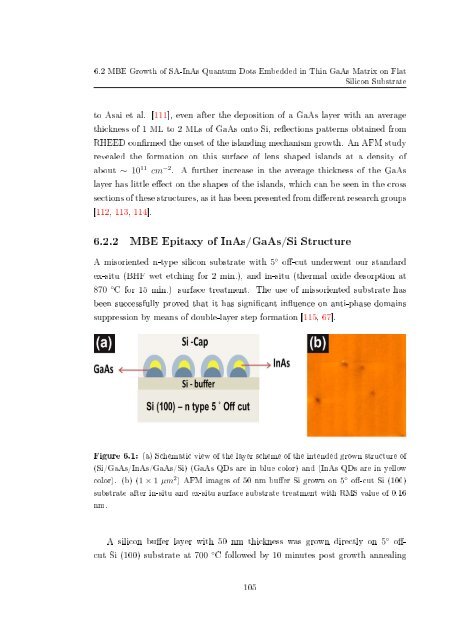
Figure 6.1: (a) Schematic view <strong>of</strong> the layer scheme <strong>of</strong> the intended grown structure <strong>of</strong><br />
(Si/GaAs/InAs/GaAs/Si) (GaAs QDs are in blue color) and (InAs QDs are in yellow<br />
color). (b) (1 × 1 µm 2 ) AFM images <strong>of</strong> 50 nm buer Si grown on 5 ◦ o-cut Si (100)<br />
substrate after in-situ and ex-situ surface substrate treatment with RMS value <strong>of</strong> 0.16<br />
nm.<br />
A silicon buer layer with 50 nm thickness was grown directly on 5 ◦ ocut<br />
Si (100) substrate at 700 ◦ C followed by 10 minutes post <strong>growth</strong> annealing<br />
105


