

Molecular beam epitaxial growth of III-V semiconductor ... - KOBRA
Molecular beam epitaxial growth of III-V semiconductor ... - KOBRA
Molecular beam epitaxial growth of III-V semiconductor ... - KOBRA

Create successful ePaper yourself
Turn your PDF publications into a flip-book with our unique Google optimized e-Paper software.
6.3 Further Results: Site-Controlled Growth <strong>of</strong> InGaAs QDs Embedded in GaAs<br />
Matrix on Pre-Patterned Silicon Substrate<br />
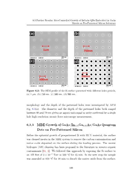
Figure 6.3: The SEM prole <strong>of</strong> the Si surface patterned with dierent holes periods,<br />
(a) 1 µm. (b) 750 nm. (c) 500 nm. (d) 200 nm.<br />
morphology and the depth <strong>of</strong> the patterned holes were investigated by AFM<br />
Fig. 6.5(a). The diameter and the depth <strong>of</strong> the patterned holes both ranged<br />
between 60 and 70 nm giving an aspect ratio equal to unity conrmed by a single<br />
hole high resolution atomic force microscopy measurement.<br />
6.3.3 MBE Growth <strong>of</strong> GaAs/In 0.15 Ga 0.85 As/GaAs Quantum<br />
Dots on Pre-Patterned Silicon<br />
Before the <strong>epitaxial</strong> <strong>growth</strong> <strong>of</strong> pre-patterned Si with <strong>III</strong>/V material, the surface<br />
was cleaned in-situ in the MBE system to remove the carbon contamination and<br />
native oxide deposited on the surface during the loading process. The atomic<br />
hydrogen (AH) cleaning has been proposed in the literature to remove organic<br />
contaminants [81, 5]. We followed this approach by exposing the Si surface to<br />
an AH ux <strong>of</strong> 3 × 10 −7 Torr at 500 ◦ C for 45 min. In the next step the sample<br />
was annealed at 850 ◦ C for 10 min to desorb the native oxide from the surface.<br />
109


