

Molecular beam epitaxial growth of III-V semiconductor ... - KOBRA
Molecular beam epitaxial growth of III-V semiconductor ... - KOBRA
Molecular beam epitaxial growth of III-V semiconductor ... - KOBRA

You also want an ePaper? Increase the reach of your titles
YUMPU automatically turns print PDFs into web optimized ePapers that Google loves.
MBE Growth <strong>of</strong> InAs and InGaAs Quantum Dots Embedded in GaAs Matrix<br />
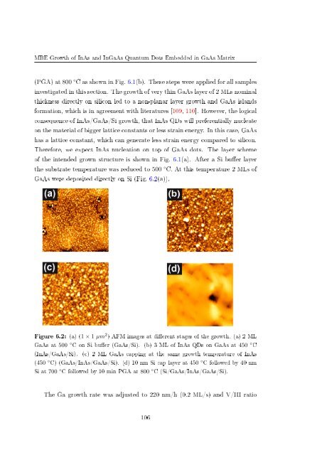
(PGA) at 800 ◦ C as shown in Fig. 6.1(b). These steps were applied for all samples<br />
investigated in this section. The <strong>growth</strong> <strong>of</strong> very thin GaAs layer <strong>of</strong> 2 MLs nominal<br />
thickness directly on silicon led to a non-planar layer <strong>growth</strong> and GaAs islands<br />
formation, which is in agreement with literatures [109, 110]. However, the logical<br />
consequence <strong>of</strong> InAs/GaAs/Si <strong>growth</strong>, that InAs QDs will preferentially nucleate<br />
on the material <strong>of</strong> bigger lattice constants or less strain energy. In this case, GaAs<br />
has a lattice constant, which can generate less strain energy compared to silicon.<br />
Therefore, we expect InAs nucleation on top <strong>of</strong> GaAs dots. The layer scheme<br />
<strong>of</strong> the intended grown structure is shown in Fig. 6.1(a). After a Si buer layer<br />
the substrate temperature was reduced to 500 ◦ C. At this temperature 2 MLs <strong>of</strong><br />
GaAs were deposited directly on Si (Fig. 6.2(a)).<br />
Figure 6.2: (a) (1 × 1 µm 2 ) AFM images at dierent stages <strong>of</strong> the <strong>growth</strong>. (a) 2 ML<br />
GaAs at 500 ◦ C on Si buer (GaAs/Si). (b) 3 ML <strong>of</strong> InAs QDs on GaAs at 450 ◦ C<br />
(InAs/GaAs/Si). (c) 2 ML GaAs capping at the same <strong>growth</strong> temperature <strong>of</strong> InAs<br />
(450 ◦ C) (GaAs/InAs/GaAs/Si). (d) 10 nm Si cap layer at 450 ◦ C followed by 40 nm<br />
Si at 700 ◦ C followed by 10 min PGA at 800 ◦ C (Si/GaAs/InAs/GaAs/Si).<br />
The Ga <strong>growth</strong> rate was adjusted to 220 nm/h (0.2 ML/s) and V/<strong>III</strong> ratio<br />
106


