

Molecular beam epitaxial growth of III-V semiconductor ... - KOBRA
Molecular beam epitaxial growth of III-V semiconductor ... - KOBRA
Molecular beam epitaxial growth of III-V semiconductor ... - KOBRA

You also want an ePaper? Increase the reach of your titles
YUMPU automatically turns print PDFs into web optimized ePapers that Google loves.
MBE Growth <strong>of</strong> InAs and InGaAs Quantum Dots Embedded in GaAs Matrix<br />
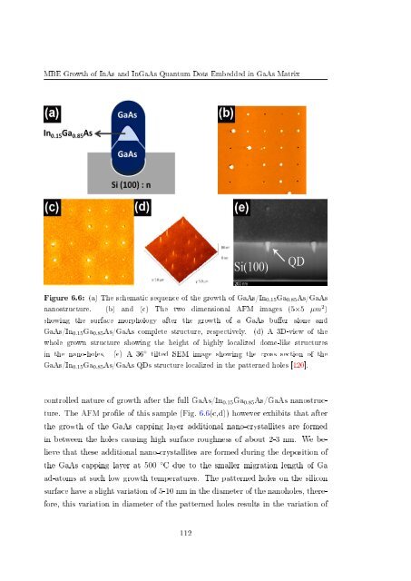
Figure 6.6: (a) The schematic sequence <strong>of</strong> the <strong>growth</strong> <strong>of</strong> GaAs/In 0.15 Ga 0.85 As/GaAs<br />
nanostructure. (b) and (c) The two dimensional AFM images (5×5 µm 2 )<br />
showing the surface morphology after the <strong>growth</strong> <strong>of</strong> a GaAs buer alone and<br />
GaAs/In 0.15 Ga 0.85 As/GaAs complete structure, respectively. (d) A 3D-view <strong>of</strong> the<br />
whole grown structure showing the height <strong>of</strong> highly localized dome-like structures<br />
in the nano-holes. (e) A 36 ◦ tilted SEM image showing the cross section <strong>of</strong> the<br />
GaAs/In 0.15 Ga 0.85 As/GaAs QDs structure localized in the patterned holes [120].<br />
controlled nature <strong>of</strong> <strong>growth</strong> after the full GaAs/In 0.15 Ga 0.85 As/GaAs nanostructure.<br />
The AFM prole <strong>of</strong> this sample (Fig. 6.6(c,d)) however exhibits that after<br />
the <strong>growth</strong> <strong>of</strong> the GaAs capping layer additional nano-crystallites are formed<br />
in between the holes causing high surface roughness <strong>of</strong> about 2-3 nm. We believe<br />
that these additional nano-crystallites are formed during the deposition <strong>of</strong><br />
the GaAs capping layer at 500 ◦ C due to the smaller migration length <strong>of</strong> Ga<br />
ad-atoms at such low <strong>growth</strong> temperatures. The patterned holes on the silicon<br />
surface have a slight variation <strong>of</strong> 5-10 nm in the diameter <strong>of</strong> the nanoholes, therefore,<br />
this variation in diameter <strong>of</strong> the patterned holes results in the variation <strong>of</strong><br />
112


