

Molecular beam epitaxial growth of III-V semiconductor ... - KOBRA
Molecular beam epitaxial growth of III-V semiconductor ... - KOBRA
Molecular beam epitaxial growth of III-V semiconductor ... - KOBRA

Create successful ePaper yourself
Turn your PDF publications into a flip-book with our unique Google optimized e-Paper software.
5.3 Results and Discussion<br />
5.3.2 Growth <strong>of</strong> InAs QDs Directly on Silicon Substrate<br />
In this section the <strong>growth</strong> conditions are: <strong>growth</strong> temperature =425 ◦ C , 2 MLs<br />
InAs coverage, V/<strong>III</strong> ratio <strong>of</strong> 20 after 15 min thermal desorption at 870 ◦ C . In<br />
the rst section, the inuence <strong>of</strong> the substrate orientation will be investigated,<br />
then the in-situ Ga surface treatment method.<br />
5.3.2.1 Dependence on Substrate Orientation<br />
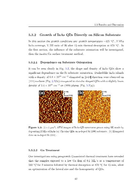
It can be seen clearly in Fig. 5.2, the shape and density <strong>of</strong> InAs QDs show a<br />
signicant dependence on the Si substrate orientation. Dashed-like InAs islands<br />
with a density <strong>of</strong> 6.8 × 10 10 cm −2 elongated in [1-10] direction were observed on<br />
(111) surfaces (Fig. 5.2(b)) compared to circular shaped QDs with a slightly lower<br />
density <strong>of</strong> 3.4 × 10 10 cm −2 on (100) planes (Fig. 5.2(a)).<br />
Figure 5.2: (1 × 1 µm 2 ) AFM images <strong>of</strong> InAs QD structures grown using SK mode by<br />
depositing 2 MLs <strong>of</strong> InAs (a) Circular QDs on n-doped Si (100) substrate. (b) Elongated<br />
dots on n-doped Si (111).<br />
5.3.2.2 Ga Treatment<br />
Our investigations using pre-<strong>growth</strong> Ga-assisted thermal treatment have revealed<br />
that the samples exposed to a low Ga ux <strong>of</strong> 0.1 ML/s at a temperature <strong>of</strong><br />
560 ◦ C for 2 minutes followed by thermal desorption at 870 ◦ C for 15 min, allow<br />
an optimization <strong>of</strong> the lateral size and the homogeneity <strong>of</strong> QDs.<br />
67


