

Molecular beam epitaxial growth of III-V semiconductor ... - KOBRA
Molecular beam epitaxial growth of III-V semiconductor ... - KOBRA
Molecular beam epitaxial growth of III-V semiconductor ... - KOBRA

Create successful ePaper yourself
Turn your PDF publications into a flip-book with our unique Google optimized e-Paper software.
MBE Growth <strong>of</strong> InAs and InGaAs Quantum Dots Embedded in GaAs Matrix<br />
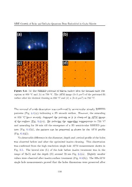
Figure 6.4: (a) The RHEED patterns <strong>of</strong> Silicon surface after the thermal oxide desorption<br />
at 850 ◦ C and (b) at 750 ◦ C. The AFM image (5×5 µm 2 ) <strong>of</strong> the patterned Si<br />
surface after the thermal cleaning at 850 ◦ C and (d) a (3×3 µm 2 ) at 750 ◦ C.<br />
The removal <strong>of</strong> oxide desorption was conrmed by semicircular streaky RHEED<br />
patterns (Fig. 6.4(a)) indicating a 2D smooth surface. However, the annealing<br />
at 850 ◦ C have severely damaged the pattern as it is observed in AFM image<br />
<strong>of</strong> the surface (Fig. 6.4(c)). By reducing the annealing temperature to 750 ◦ C<br />
and annealing for 30 min till the emergence <strong>of</strong> a 2D semicircular RHEED pattern<br />
(Fig. 6.4(b)), the pattern can be preserved as shown by the AFM prole<br />
(Fig. 6.4(d)).<br />
No detectable dierence in the diameter, depth and vertical prole <strong>of</strong> the holes<br />
was observed before and after the optimized in-situ cleaning. This observation<br />
was conrmed from the high resolution single hole AFM measurement shown in<br />
Fig. 6.5. The lateral size (L) <strong>of</strong> the hole before in-situ treatment was in the<br />
range <strong>of</strong> 70-75 and the depth (D) around 70 nm Fig. 6.5(a). Slightly smaller<br />
values were observed after in-situ surface treatment (Fig. 6.5(b)). The HR-AFM<br />
single hole measurements proved that the holes dimensions were preserved after<br />
110


