

Molecular beam epitaxial growth of III-V semiconductor ... - KOBRA
Molecular beam epitaxial growth of III-V semiconductor ... - KOBRA
Molecular beam epitaxial growth of III-V semiconductor ... - KOBRA

You also want an ePaper? Increase the reach of your titles
YUMPU automatically turns print PDFs into web optimized ePapers that Google loves.
Hetero<strong>epitaxial</strong> Growth <strong>of</strong> <strong>III</strong>-V Semiconductor on Silicon Substrates<br />
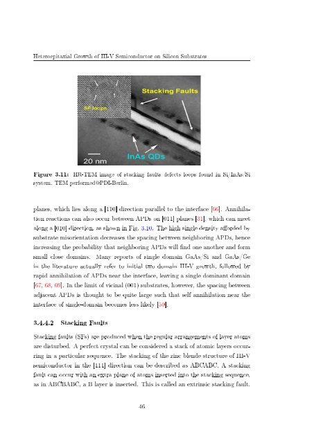
Figure 3.11:<br />
HR-TEM image <strong>of</strong> stacking faults defects loops found in Si/InAs/Si<br />
system. TEM performed@PDI-Berlin.<br />
planes, which lies along a [110] direction parallel to the interface [66]. Annihilation<br />
reactions can also occur between APDs on [011] planes [31], which can meet<br />
along a [010] direction, as shown in Fig. 3.10. The high single density aorded by<br />
substrate misorientation decreases the spacing between neighboring APDs, hence<br />
increasing the probability that neighboring APDs will nd one another and form<br />
small close domains. Many reports <strong>of</strong> single domain GaAs/Si and GaAs/Ge<br />
in the literature actually refer to initial two domain <strong>III</strong>-V <strong>growth</strong>, followed by<br />
rapid annihilation <strong>of</strong> APDs near the interface, leaving a single dominant domain<br />
[67, 68, 69]. In the limit <strong>of</strong> vicinal (001) substrates, however, the spacing between<br />
adjacent APDs is thought to be quite large such that self annihilation near the<br />
interface <strong>of</strong> single-domain becomes less likely [50].<br />
3.4.4.2 Stacking Faults<br />
Stacking faults (SFs) are produced when the regular arrangements <strong>of</strong> layer atoms<br />
are disturbed. A perfect crystal can be considered a stack <strong>of</strong> atomic layers occurring<br />
in a particular sequence. The stacking <strong>of</strong> the zinc blende structure <strong>of</strong> <strong>III</strong>-V<br />
<strong>semiconductor</strong> in the [111] direction can be described as ABCABC. A stacking<br />
fault can occur with an extra plane <strong>of</strong> atoms inserted into the stacking sequence,<br />
as in ABCBABC, a B layer is inserted. This is called an extrinsic stacking fault.<br />
46


