

Molecular beam epitaxial growth of III-V semiconductor ... - KOBRA
Molecular beam epitaxial growth of III-V semiconductor ... - KOBRA
Molecular beam epitaxial growth of III-V semiconductor ... - KOBRA

Create successful ePaper yourself
Turn your PDF publications into a flip-book with our unique Google optimized e-Paper software.
Optimization <strong>of</strong> MEE and MBE <strong>growth</strong> <strong>of</strong> GaP Buer on Silicon Substrate<br />
for the Ga-initiated MEE <strong>growth</strong> recipe with RMS value <strong>of</strong> 0.51 nm which is in<br />
agreement with the literatures [133, 49]. As a result the Ga-initiated <strong>growth</strong> with<br />
the time sequence <strong>of</strong> 10 s Ga/ 4 s stop/10 s P 2 /60 s was chosen for all following<br />
MEE runs. In the next subsections MEE <strong>growth</strong> mode was optimized for other<br />
<strong>growth</strong> parameters like <strong>growth</strong> temperature and V/<strong>III</strong> ratio.<br />
7.4.1 MEE-GaP Growth Temperature<br />
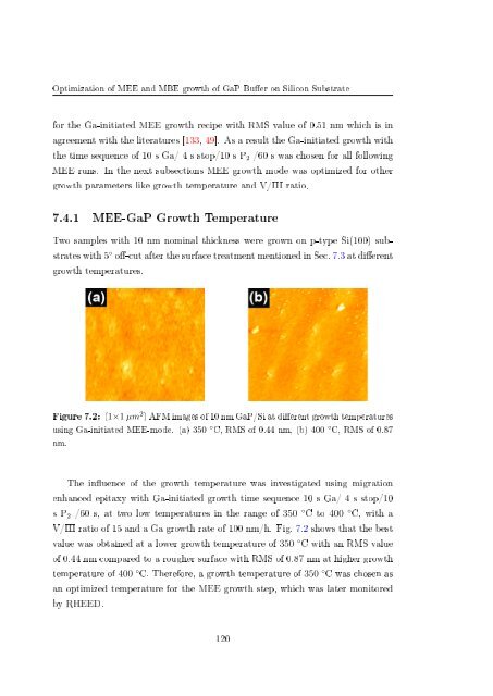
Two samples with 10 nm nominal thickness were grown on p-type Si(100) substrates<br />
with 5 ◦ o-cut after the surface treatment mentioned in Sec. 7.3 at dierent<br />
<strong>growth</strong> temperatures.<br />
Figure 7.2: (1×1 µm 2 ) AFM images <strong>of</strong> 10 nm GaP/Si at dierent <strong>growth</strong> temperatures<br />
using Ga-initiated MEE-mode. (a) 350 ◦ C, RMS <strong>of</strong> 0.44 nm, (b) 400 ◦ C, RMS <strong>of</strong> 0.87<br />
nm.<br />
The inuence <strong>of</strong> the <strong>growth</strong> temperature was investigated using migration<br />
enhanced epitaxy with Ga-initiated <strong>growth</strong> time sequence 10 s Ga/ 4 s stop/10<br />
s P 2 /60 s, at two low temperatures in the range <strong>of</strong> 350 ◦ C to 400 ◦ C, with a<br />
V/<strong>III</strong> ratio <strong>of</strong> 15 and a Ga <strong>growth</strong> rate <strong>of</strong> 100 nm/h. Fig. 7.2 shows that the best<br />
value was obtained at a lower <strong>growth</strong> temperature <strong>of</strong> 350 ◦ C with an RMS value<br />
<strong>of</strong> 0.44 nm compared to a rougher surface with RMS <strong>of</strong> 0.87 nm at higher <strong>growth</strong><br />
temperature <strong>of</strong> 400 ◦ C. Therefore, a <strong>growth</strong> temperature <strong>of</strong> 350 ◦ C was chosen as<br />
an optimized temperature for the MEE <strong>growth</strong> step, which was later monitored<br />
by RHEED.<br />
120


