

Molecular beam epitaxial growth of III-V semiconductor ... - KOBRA
Molecular beam epitaxial growth of III-V semiconductor ... - KOBRA
Molecular beam epitaxial growth of III-V semiconductor ... - KOBRA

You also want an ePaper? Increase the reach of your titles
YUMPU automatically turns print PDFs into web optimized ePapers that Google loves.
MBE Growth <strong>of</strong> Self-Assembled InAs and InGaAs Quantum Dots Embedded in<br />
Silicon Matrix<br />
and V-SF formation above and around the InAs QDs have been observed after<br />
the rst PGA cycle at 700 ◦ C. Nevertheless the QDs in Si voids will also evaporate,<br />
but the vapor is conned in the voids, evolved nally to nearly spherical<br />
QD shape. A further Si capping at 700 ◦ C has inuence on Si surface reconstruction<br />
and circular-voids kinetics. A localized circular-voids formation above the<br />
semi-coherent InAs QDs layer only has been observed after the nal Si capping<br />
step. The second PGA cycle at 800 ◦ C proved to have strong impact on circularvoids<br />
kinetics and Si <strong>growth</strong> quality, through total re-crystallization and melting<br />
<strong>of</strong> the whole structure and new atomic arrangement. A high quality (defect-free)<br />
Si matrix <strong>growth</strong> with voids and V-SF free has been observed after the second<br />
PGA cycle at 800 ◦ C conrming the proposed <strong>growth</strong> model in Fig. 5.21. Strain<br />
analysis conrmed almost fully relaxed QDs. However, These QDs are relaxed via<br />
the creation <strong>of</strong> mist dislocation loops that are restricted in the InAs/Si interface<br />
region, whereas the Si matrix is (extended) defect-free and with no detectable<br />
strain gradient. However, in some cases few SFs and MTs are observed to form<br />
only inside the dots.<br />
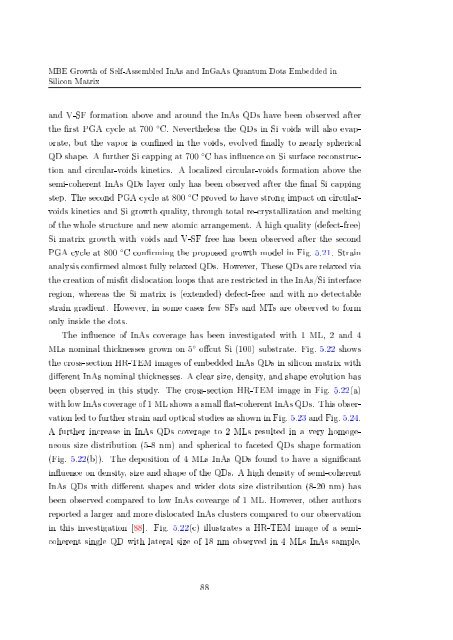
The inuence <strong>of</strong> InAs coverage has been investigated with 1 ML, 2 and 4<br />
MLs nominal thicknesses grown on 5 ◦ ocut Si (100) substrate. Fig. 5.22 shows<br />
the cross-section HR-TEM images <strong>of</strong> embedded InAs QDs in silicon matrix with<br />
dierent InAs nominal thicknesses. A clear size, density, and shape evolution has<br />
been observed in this study. The cross-section HR-TEM image in Fig. 5.22(a)<br />
with low InAs coverage <strong>of</strong> 1 ML shows a small at-coherent InAs QDs. This observation<br />
led to further strain and optical studies as shown in Fig. 5.23 and Fig. 5.24.<br />
A further increase in InAs QDs coverage to 2 MLs resulted in a very homogeneous<br />
size distribution (5-8 nm) and spherical to faceted QDs shape formation<br />
(Fig. 5.22(b)). The deposition <strong>of</strong> 4 MLs InAs QDs found to have a signicant<br />
inuence on density, size and shape <strong>of</strong> the QDs. A high density <strong>of</strong> semi-coherent<br />
InAs QDs with dierent shapes and wider dots size distribution (8-20 nm) has<br />
been observed compared to low InAs covearge <strong>of</strong> 1 ML. However, other authors<br />
reported a larger and more dislocated InAs clusters compared to our observation<br />
in this investigation [88]. Fig. 5.22(c) illustrates a HR-TEM image <strong>of</strong> a semicoherent<br />
single QD with lateral size <strong>of</strong> 18 nm observed in 4 MLs InAs sample.<br />
88


