

Molecular beam epitaxial growth of III-V semiconductor ... - KOBRA
Molecular beam epitaxial growth of III-V semiconductor ... - KOBRA
Molecular beam epitaxial growth of III-V semiconductor ... - KOBRA

You also want an ePaper? Increase the reach of your titles
YUMPU automatically turns print PDFs into web optimized ePapers that Google loves.
5.4 Self-Assembled InAs QDs Embedded in Si Matrix<br />
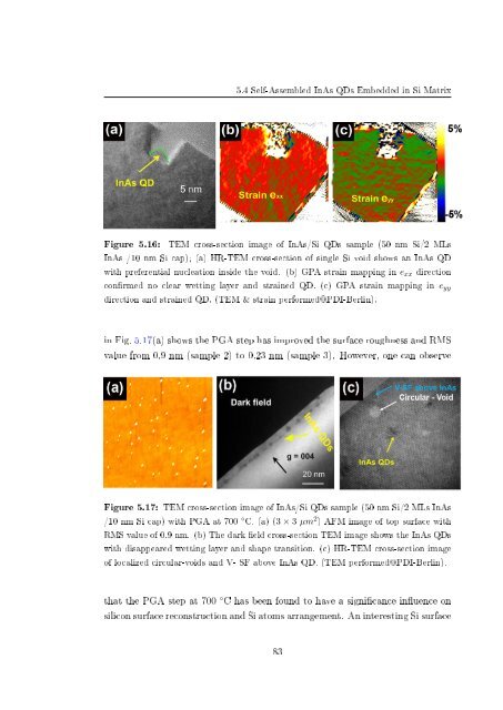
Figure 5.16:<br />
TEM cross-section image <strong>of</strong> InAs/Si QDs sample (50 nm Si/2 MLs<br />
InAs /10 nm Si cap); (a) HR-TEM cross-section <strong>of</strong> single Si void shows an InAs QD<br />
with preferential nucleation inside the void. (b) GPA strain mapping in e xx direction<br />
conrmed no clear wetting layer and strained QD. (c) GPA strain mapping in e yy<br />
direction and strained QD. (TEM & strain performed@PDI-Berlin).<br />
in Fig. 5.17(a) shows the PGA step has improved the surface roughness and RMS<br />
value from 0.9 nm (sample 2) to 0.23 nm (sample 3). However, one can observe<br />
Figure 5.17: TEM cross-section image <strong>of</strong> InAs/Si QDs sample (50 nm Si/2 MLs InAs<br />
/10 nm Si cap) with PGA at 700 ◦ C. (a) (3 × 3 µm 2 ) AFM image <strong>of</strong> top surface with<br />
RMS value <strong>of</strong> 0.9 nm. (b) The dark eld cross-section TEM image shows the InAs QDs<br />
with disappeared wetting layer and shape transition. (c) HR-TEM cross-section image<br />
<strong>of</strong> localized circular-voids and V- SF above InAs QD. (TEM performed@PDI-Berlin).<br />
that the PGA step at 700 ◦ C has been found to have a signicance inuence on<br />
silicon surface reconstruction and Si atoms arrangement. An interesting Si surface<br />
83


