

Molecular beam epitaxial growth of III-V semiconductor ... - KOBRA
Molecular beam epitaxial growth of III-V semiconductor ... - KOBRA
Molecular beam epitaxial growth of III-V semiconductor ... - KOBRA

You also want an ePaper? Increase the reach of your titles
YUMPU automatically turns print PDFs into web optimized ePapers that Google loves.
5.4 Self-Assembled InAs QDs Embedded in Si Matrix<br />
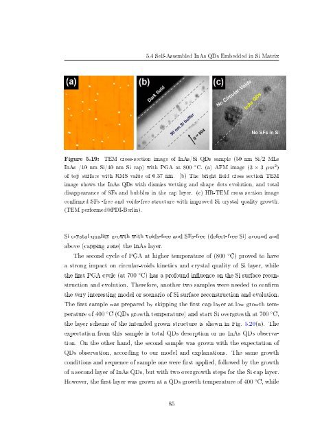
Figure 5.19:<br />
TEM cross-section image <strong>of</strong> InAs/Si QDs sample (50 nm Si/2 MLs<br />
InAs /10 nm Si/40 nm Si cap) with PGA at 800 ◦ C. (a) AFM image (3 × 3 µm 2 )<br />
<strong>of</strong> top surface with RMS value <strong>of</strong> 0.37 nm. (b) The bright eld cross section TEM<br />
image shows the InAs QDs with dismiss wetting and shape dots evolution, and total<br />
disappearance <strong>of</strong> SFs and bubbles in the cap layer. (c) HR-TEM cross section image<br />
conrmed SFs -free and voids-free structure with improved Si crystal quality <strong>growth</strong>.<br />
(TEM performed@PDI-Berlin).<br />
Si crystal quality <strong>growth</strong> with voids-free and SFs-free (defect-free Si) around and<br />
above (capping zone) the InAs layer.<br />
The second cycle <strong>of</strong> PGA at higher temperature <strong>of</strong> (800 ◦ C) proved to have<br />
a strong impact on circular-voids kinetics and crystal quality <strong>of</strong> Si layer, while<br />
the rst PGA cycle (at 700 ◦ C) has a pr<strong>of</strong>ound inuence on the Si surface reconstruction<br />
and evolution. Therefore, another two samples were needed to conrm<br />
the very interesting model or scenario <strong>of</strong> Si surface reconstruction and evolution.<br />
The rst sample was prepared by skipping the rst cap layer at low <strong>growth</strong> temperature<br />
<strong>of</strong> 400 ◦ C (QDs <strong>growth</strong> temperature) and start Si over<strong>growth</strong> at 700 ◦ C,<br />
the layer scheme <strong>of</strong> the intended grown structure is shown in Fig. 5.20(a). The<br />
expectation from this sample is total QDs desorption or no InAs QDs observation.<br />
On the other hand, the second sample was grown with the expectation <strong>of</strong><br />
QDs observation, according to our model and explanations. The same <strong>growth</strong><br />
conditions and sequence <strong>of</strong> sample one were rst applied, followed by the <strong>growth</strong><br />
<strong>of</strong> a second layer <strong>of</strong> InAs QDs, but with two over<strong>growth</strong> steps for the Si cap layer.<br />
However, the rst layer was grown at a QDs <strong>growth</strong> temperature <strong>of</strong> 400 ◦ C, while<br />
85


